Table of Contents
1. HW 1: Tools Introduction
CMPE 316 UMBC
Prof. Ryan Robucci
students working in identified pairs are allowed to collaborate without restriction on this assignment but each students should install the software and complete steps on their computer and submit independently. Submission instructions are TBD, but expect them soon (back up your work in the meantime).
1.0.1. Objective
The objective of this lab is to learn the fundamental components of the Xilinx FGPA tools required to enter and assemble HDL code using a schematic entry tool and program an FPGA. This includes integrating HDL into a schematic, as well as creating and updating symbols.
1.0.2. Prerequisite
- Install Xilinx Vivado and drivers
In this lab you will program an FPGA to display a rectangle on a monitor using a VGA cable. You will first create an implementation with an error in it and view the results. You will then modify the code, update the symbol in the schematic, and wire the schematic correctly to control the color of the rectangle using switches.
1.0.3. Tutorial Steps
- Start Xilinx Vivado:
source /opt/Xilinx/Vivado/2023.2/settings64.shvivado
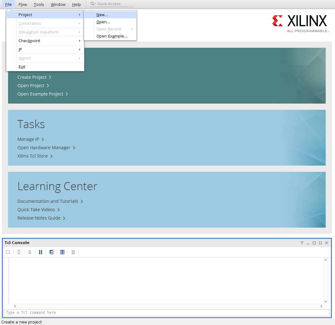
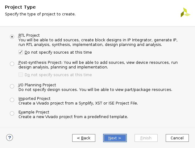
- Create New Project
In main window menu: File->New Project…
- …
- …
- …
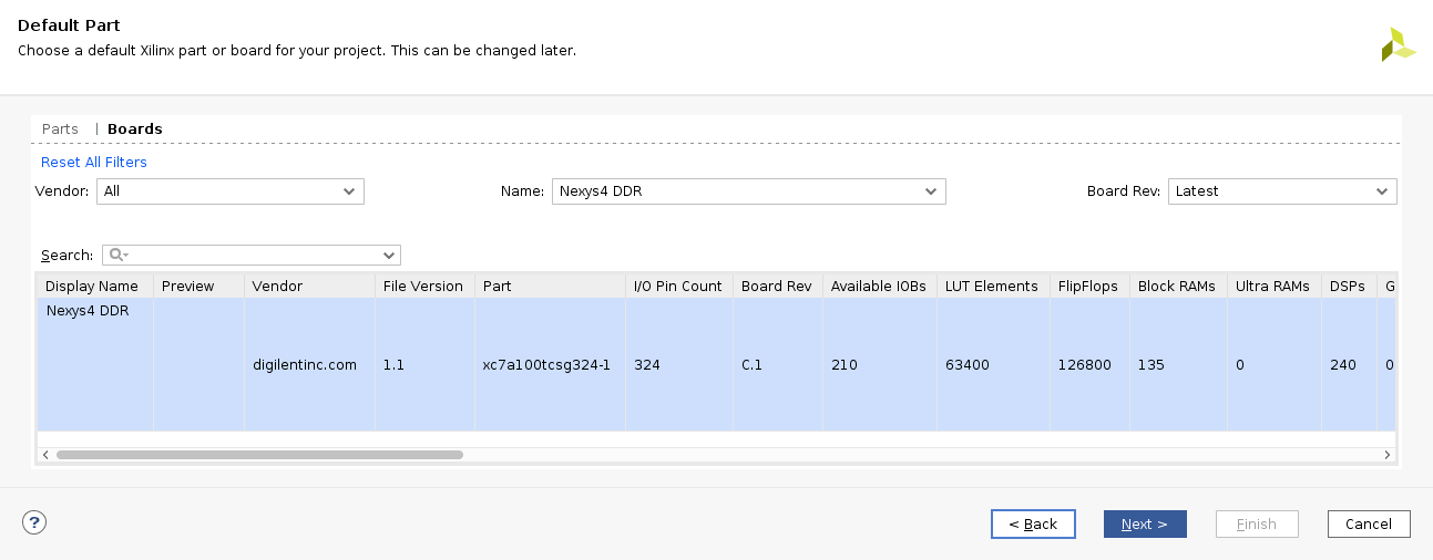
- You'll now need to enter information about the FPGA. You can look in
the reference manual to find the information
https://reference.digilentinc.com/reference/programmable-logic/nexys-4-ddr/reference-manual
or you can use the board support files if you downloaded and
installed them:
- The next screen shows a summary.
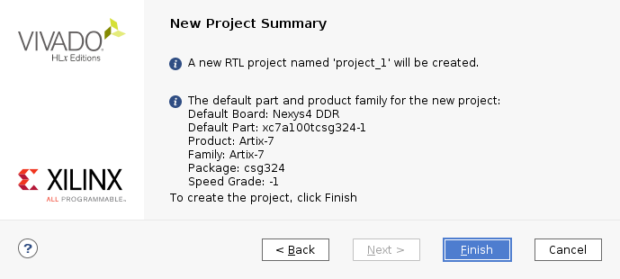
- Hit Finish.
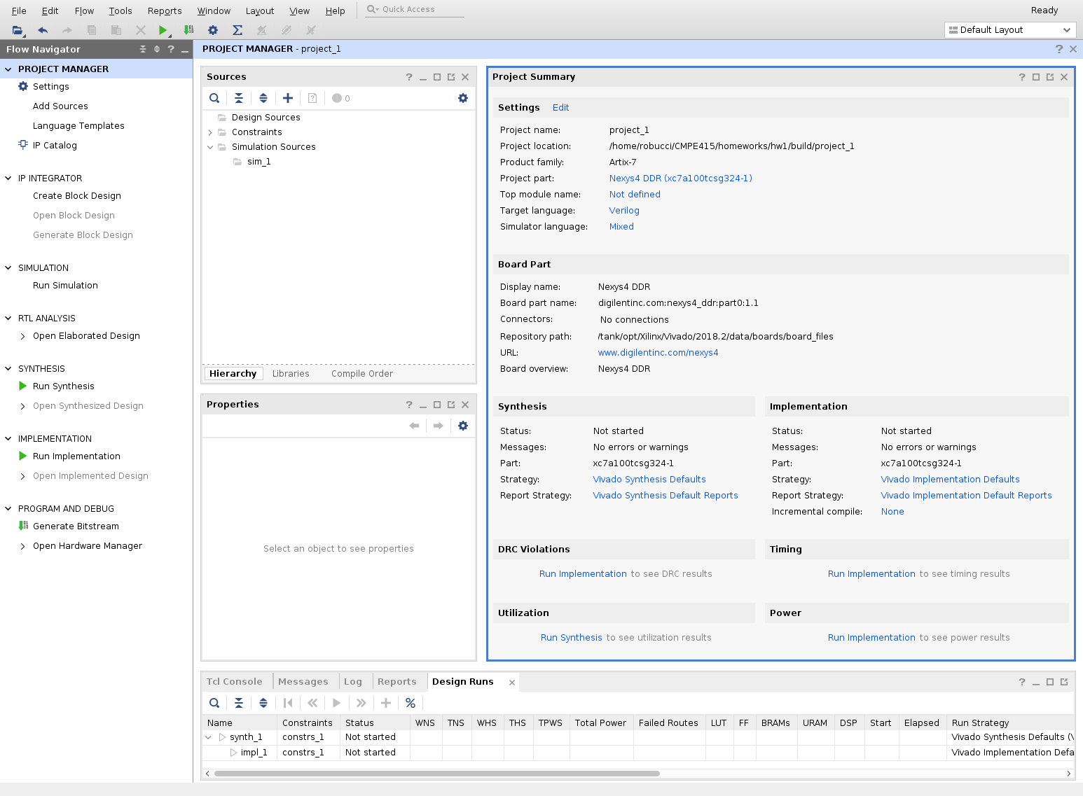
Result:
- Download an HDL Module, Modify and Add to project
- Select a free HDL description of implementation of a vga module to a
temporary directory or to your project directory. Our other module
will be implmented using Verilog, but we can integrate Verilog and
VHDL modules together in the schematic if desired. Here are examples
of the type of vga modules for which you are looking. Make sure to
respect any restrictions the authors place on copyrighted code that
you use.
- http://web.mit.edu/6.111/www/f2005/code/jtag2mem_6111/vga_sync.v Verilog implementation (I'll use this one.)
- http://www.ece.gatech.edu/academic/courses/fpga/Xilinx/downloads/vga_sync.vhd VHDL implementation (handles blanking internally)
- http://jjackson.eng.ua.edu/courses/ece480/assignments/vga_sync.vhd VHDL implementation with parameters to set various resolutions (also, implements a “videoon” signal instead of a “blank” signal )
Download the code to a src directory
mkdir ~/CMPE316/homeworks/hw1/src
cd ~/CMPE316/homeworks/hw1/src
wget http://web.mit.edu/6.111/www/f2005/code/jtag2mem_6111/vga_sync.v
Modify code to work with a 100-MHz clock change the 1-bit counter to a 2-bit counter
// pixel clock: 25Mhz = 40ns (clk/2)
reg pcount;      // used to generate pixel clock
wire en = (pcount == 0);
always @ (posedge clk) pcount <= ~pcount;
assign pix_clk = en;
becomes
// pixel clock: 25Mhz = 40ns (clk/4)
reg [1:0] pcount;        // used to generate pixel clock
wire en = (pcount == 0);
always @ (posedge clk) pcount <= pcount + 1 ;
assign pix_clk = en;
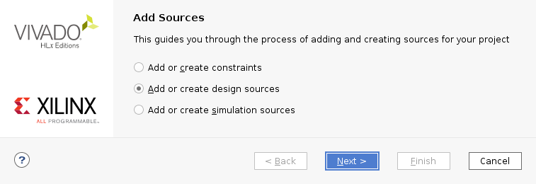
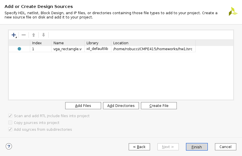
- Add the source to the project using File-> Add
Sources…
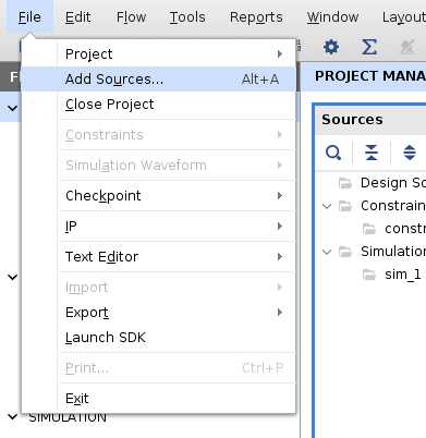
- We will use the second option:
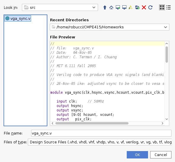
Click Add Files
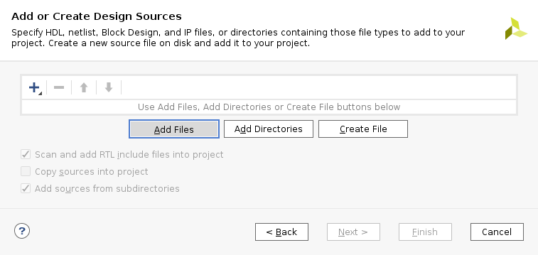
navigate to src dir (e.g. /home/robucci/CMPE316/homeworks/hw1/src) and select the vgasync.v file
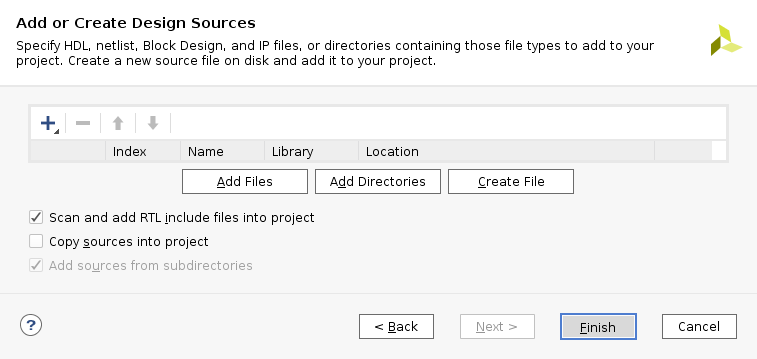
You now have a new Design Source listed
- Select a free HDL description of implementation of a vga module to a
temporary directory or to your project directory. Our other module
will be implmented using Verilog, but we can integrate Verilog and
VHDL modules together in the schematic if desired. Here are examples
of the type of vga modules for which you are looking. Make sure to
respect any restrictions the authors place on copyrighted code that
you use.
- Create VGA Rectangle Generator Verilog Module
We will now create a second source file.
- Add a source as before, but this time select Create
File
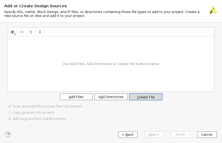
- …
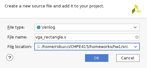
- …
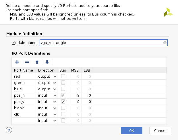
- You should now have a shell created with port definitions. Double
click the file to edit it and make the modifications below
Set the reg, green, and blue outputs as reg. Implementing registers avoids glitching (not that it is critical here). change
         output red,
         output green,
         output blue,
to
         output reg red,
         output reg green,
         output reg blue,
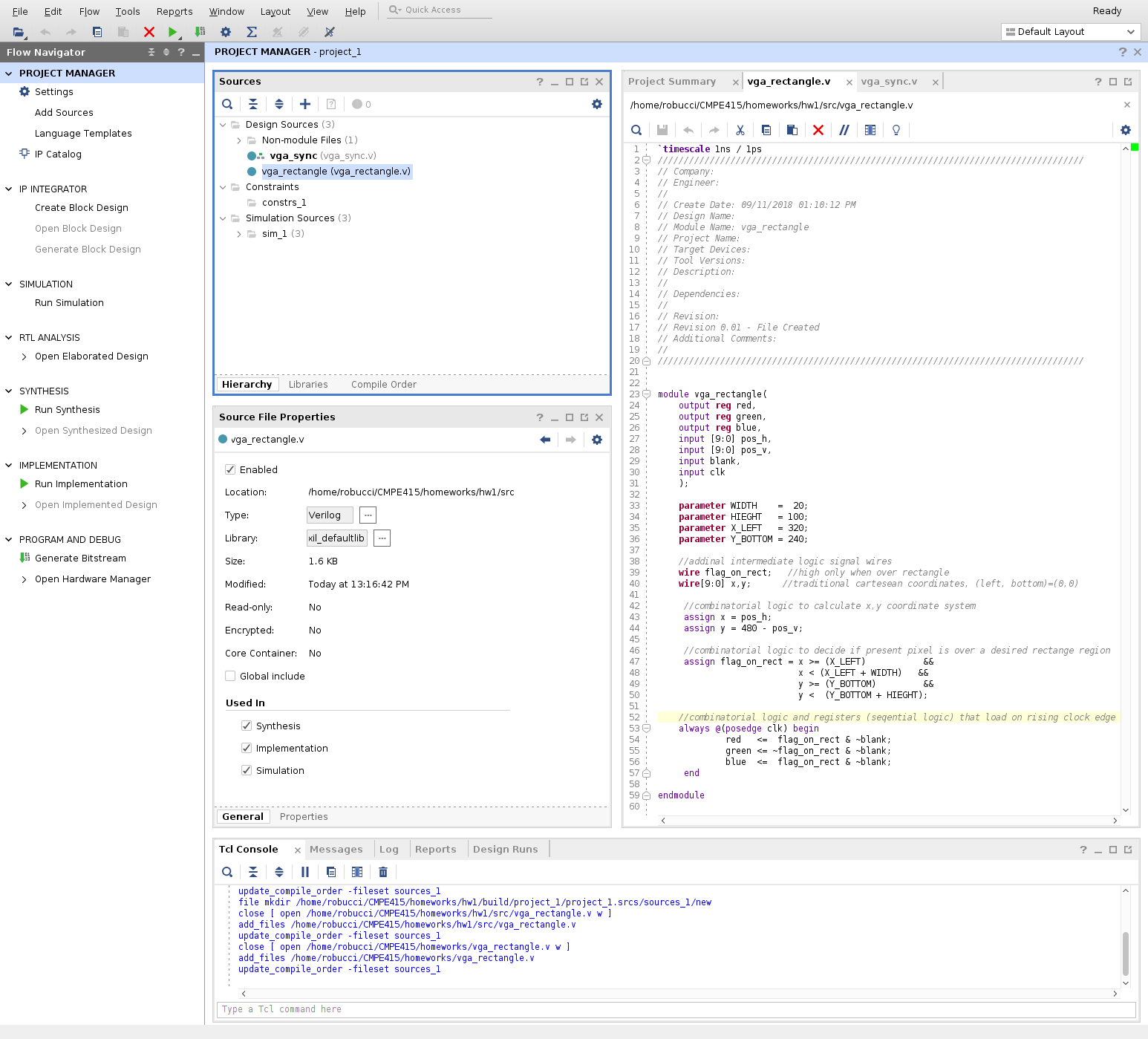
Add the following module code which takes the coodinates as inputs and outputs the color:
parameter WIDTH = 20; parameter HIEGHT = 100; parameter X_LEFT = 320; parameter Y_BOTTOM = 240; //addinal intermediate logic signal wires wire flag_on_rect; //high only when over rectangle wire[9:0] x,y; //traditional cartesean coordinates, (left, bottom)=(0,0) //combinatorial logic to calculate x,y coordinate system assign x = pos_h; assign y = 480 - pos_v; //combinatorial logic to decide if present pixel is over a desired rectange region assign flag_on_rect = x >= (X_LEFT) && x < (X_LEFT + WIDTH) && y >= (Y_BOTTOM) && y < (Y_BOTTOM + HIEGHT); //combinatorial logic and registers (seqential logic) that load on rising clock edge always @(posedge clk) begin red <= flag_on_rect &~blank; green <= ~flag_on_rect &~blank; blue <= flag_on_rect &~blank; end
- Add a source as before, but this time select Create
File
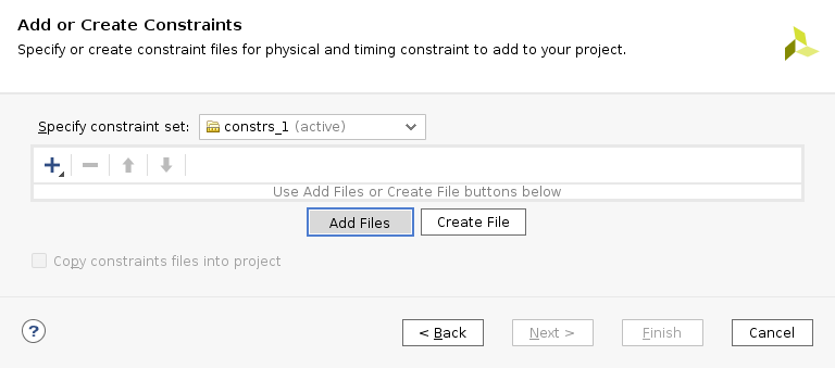
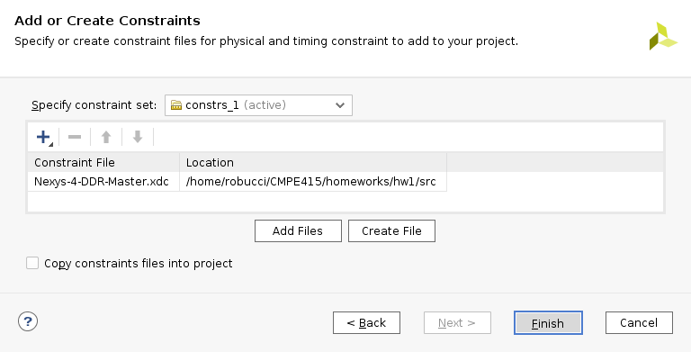
- Obtain, edit, and add a Contraints File to Specify Pin Locations, Voltage, and Clock Rate Compatable with the Board
The board that we are using can be considered as a reference board for learning to use the type of FPGA from Xilinx. Usually such boards come with a reference manual and what is called a constraint file that describes where pins are connected on the FPGA and the frequency the input clock generated on the board.
The provided file from one of these locations:
- https://reference.digilentinc.com/reference/programmable-logic/nexys-4-ddr/start#additional_resources
- wget https://raw.githubusercontent.com/Digilent/digilent-xdc/master/Nexys-4-DDR-Master.xdc
Place the file in your src directory
Uncomment the following lines setproperty lines in the file:
## Clock signal
set_property -dict { PACKAGE_PIN E3    IOSTANDARD LVCMOS33 } [get_ports { CLK100MHZ }]; #IO_L12P_T1_MRCC_35 Sch=clk100mhz
create_clock -add -name sys_clk_pin -period 10.00 -waveform {0 5} [get_ports {CLK100MHZ}];
##VGA Connector set_property -dict { PACKAGE_PIN A3 IOSTANDARD LVCMOS33 } [get_ports { VGA_R[0] }]; #IO_L8N_T1_AD14N_35 Sch=vga_r[0] set_property -dict { PACKAGE_PIN B4 IOSTANDARD LVCMOS33 } [get_ports { VGA_R[1] }]; #IO_L7N_T1_AD6N_35 Sch=vga_r[1] set_property -dict { PACKAGE_PIN C5 IOSTANDARD LVCMOS33 } [get_ports { VGA_R[2] }]; #IO_L1N_T0_AD4N_35 Sch=vga_r[2] set_property -dict { PACKAGE_PIN A4 IOSTANDARD LVCMOS33 } [get_ports { VGA_R[3] }]; #IO_L8P_T1_AD14P_35 Sch=vga_r[3] set_property -dict { PACKAGE_PIN C6 IOSTANDARD LVCMOS33 } [get_ports { VGA_G[0] }]; #IO_L1P_T0_AD4P_35 Sch=vga_g[0] set_property -dict { PACKAGE_PIN A5 IOSTANDARD LVCMOS33 } [get_ports { VGA_G[1] }]; #IO_L3N_T0_DQS_AD5N_35 Sch=vga_g[1] set_property -dict { PACKAGE_PIN B6 IOSTANDARD LVCMOS33 } [get_ports { VGA_G[2] }]; #IO_L2N_T0_AD12N_35 Sch=vga_g[2] set_property -dict { PACKAGE_PIN A6 IOSTANDARD LVCMOS33 } [get_ports { VGA_G[3] }]; #IO_L3P_T0_DQS_AD5P_35 Sch=vga_g[3] set_property -dict { PACKAGE_PIN B7 IOSTANDARD LVCMOS33 } [get_ports { VGA_B[0] }]; #IO_L2P_T0_AD12P_35 Sch=vga_b[0] set_property -dict { PACKAGE_PIN C7 IOSTANDARD LVCMOS33 } [get_ports { VGA_B[1] }]; #IO_L4N_T0_35 Sch=vga_b[1] set_property -dict { PACKAGE_PIN D7 IOSTANDARD LVCMOS33 } [get_ports { VGA_B[2] }]; #IO_L6N_T0_VREF_35 Sch=vga_b[2] set_property -dict { PACKAGE_PIN D8 IOSTANDARD LVCMOS33 } [get_ports { VGA_B[3] }]; #IO_L4P_T0_35 Sch=vga_b[3] set_property -dict { PACKAGE_PIN B11 IOSTANDARD LVCMOS33 } [get_ports { VGA_HS }]; #IO_L4P_T0_15 Sch=vga_hs set_property -dict { PACKAGE_PIN B12 IOSTANDARD LVCMOS33 } [get_ports { VGA_VS }]; #IO_L3N_T0_DQS_AD1N_15 Sch=vga_vs
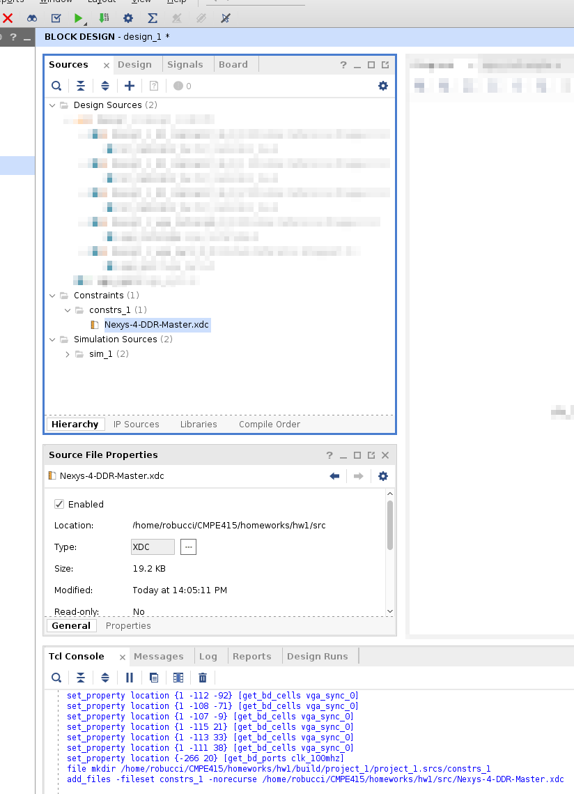
Add the constraints file from the src directory.

- Glue Logic 1-bit to 4-bit output
You can note that the vgar,vgag, and vgab are 4 bits each, but our vgarectangle reg,green, and blue outputs are 1-bit.
Before we connect modules and FPGA pins, lets create some "glue logic" that expands a 1-bit to 4-bit
Create another module called bitreplicator4x (be sure to store it in the src directory) with a 1-bit input "dIn" and a 4-bit output dOut. Add one line of code to the module:
assign dOut = {4{dIn}};
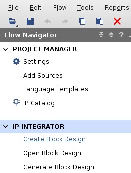
- Create Top Level Design
We now want to create a top level design with modules connected using the following I/O names at the top level CLK100MHZ, VGAR,VGAG,VGAB so that they match the provided constraints file and thus what you would find in the board documentation.
Two options are to create a Verilog file directly, and the second it to use a schematic tool to draw the design then generate the top level Verilog for it. We'll do the latter since it effectively shows both concepts.
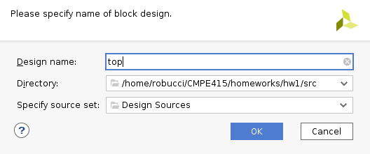
We'll add a block design using Create Block Design
We'll choose a name "top" for the design and place it in the src directory
There is now a top.pd in your sources and a schematic waiting to be draw on the right:
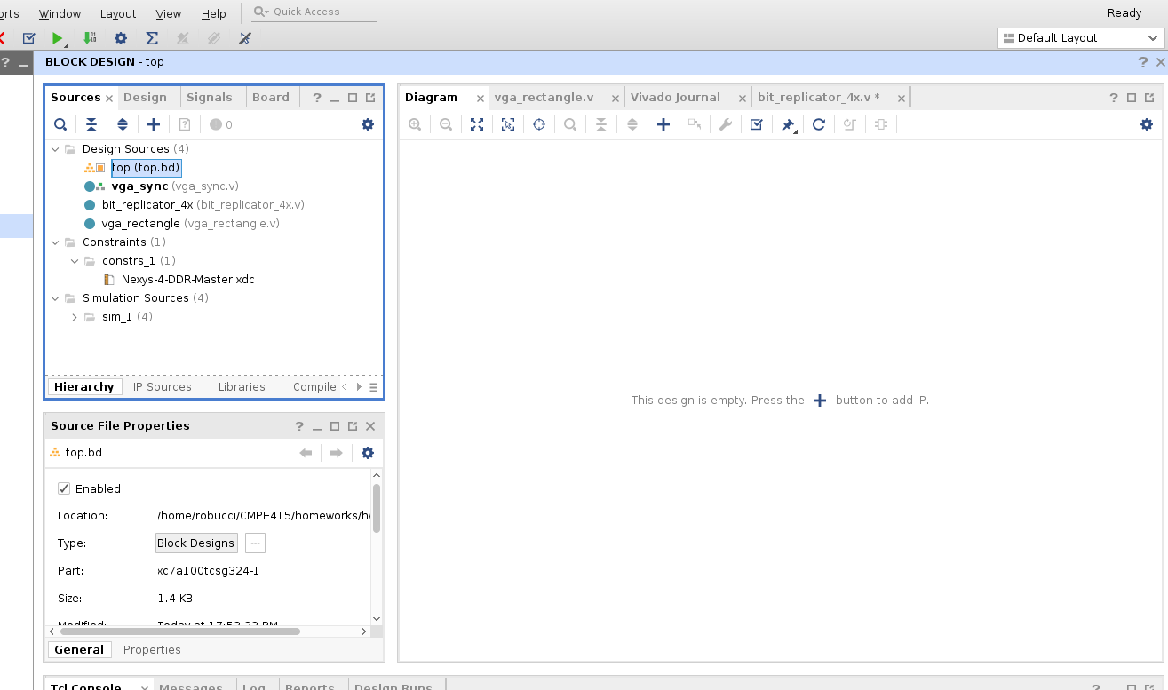
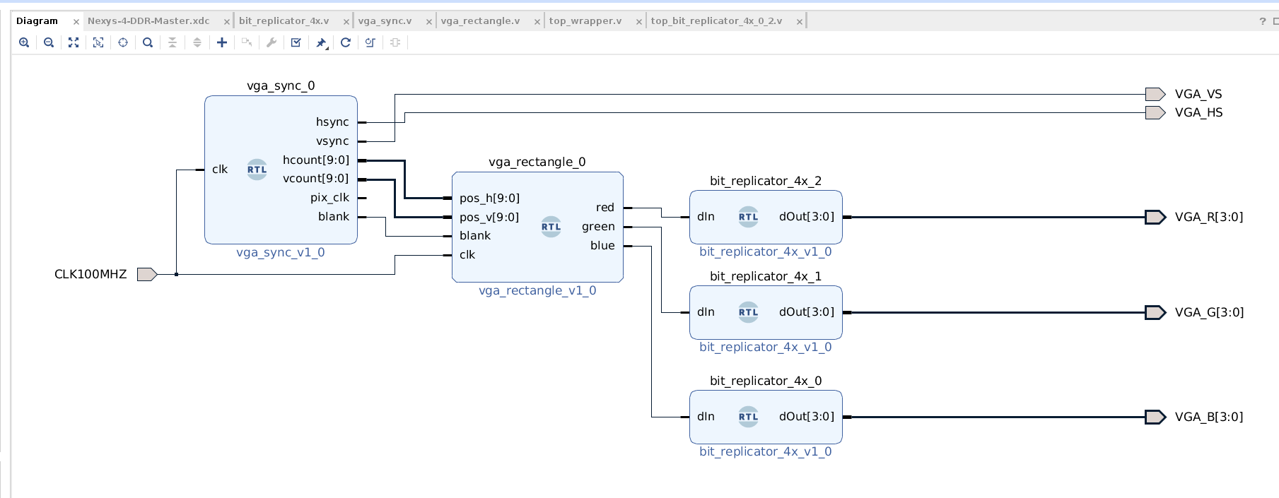
To add your modules, and pins/ports use the right click menu within the Diagram area:
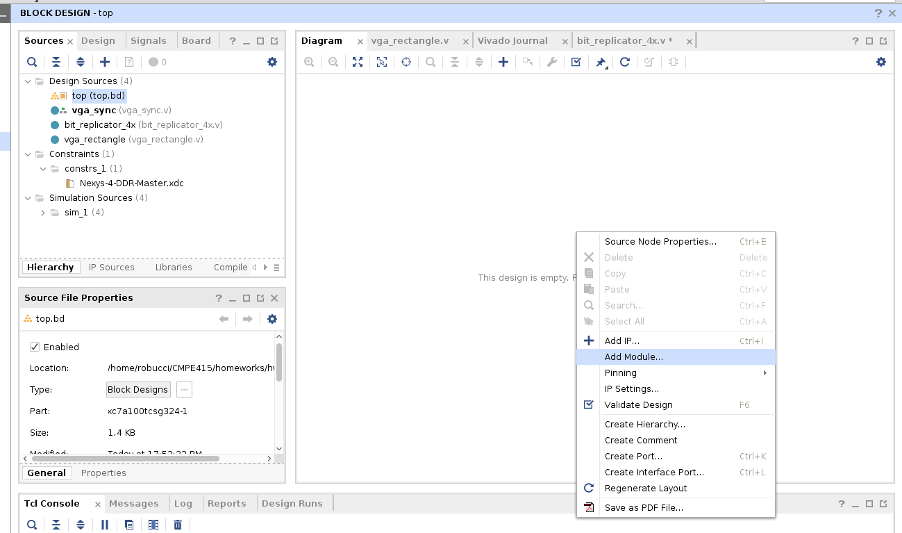
First add the
vga_sync, then thevga_rectangle, then three of thebit_replicator_4x(can also use copy and paste get three)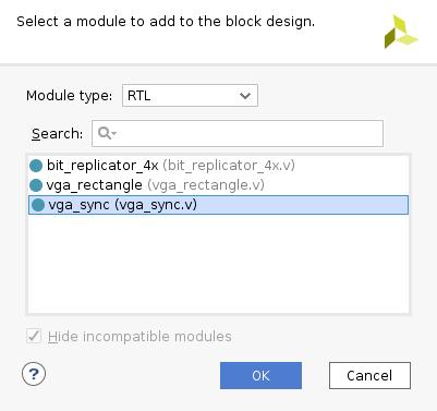 block diagram design
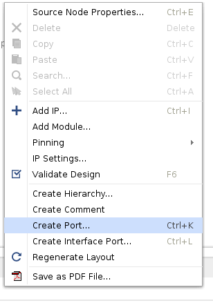
Pins/port can be added using the same menu. Create
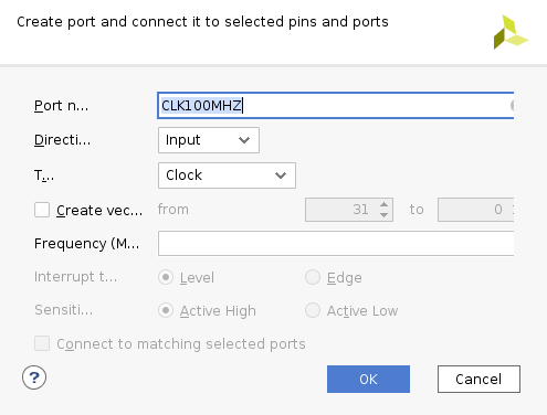
- input clock:
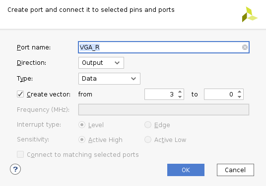
CLK100MHZ - output data 3 downto 0 :
VGA_R,VGA_G,VGA_B - output data
VGA_HS,VGA_VS
For
VGA_GandVGA_B, copy and pasteVGA_Rthen change the name using the property box (modules not show in this screenshot):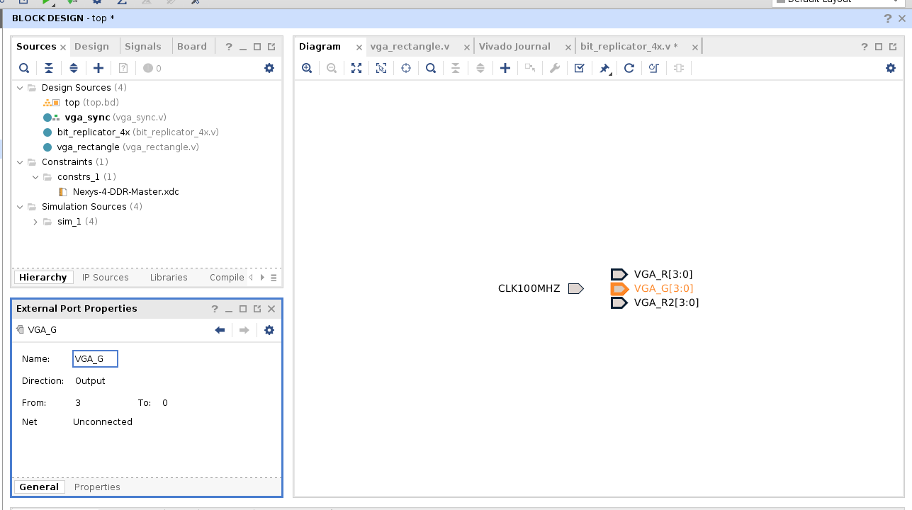
Here is a final schematic:
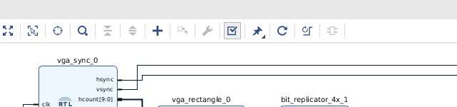
You can validate the design using the checkbox:
To make actually create our top level design, Vivado seems to requires a Verilog file, so right click the top.bd and select Create HDL Wrapper
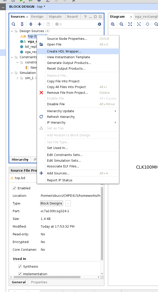
I WOULD HAVE asked you to right-click the
top_wrapperand select Set as Top, but if you wait a moment Vivado figures this out and moves the top indicator icon (green box above two gray boxes). - input clock:
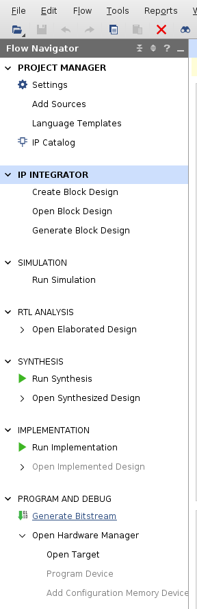
- Synthesize, Implement, and Generate Programming File
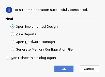
You can now click Generate Bitstream on the left, found right under Program and Debug
- Use the defaults and ok-click through the next dialog.
- You'll note progress/status/messaage in the upper-right corner of the Vivado window.
- “Synthesize” and “Implement Design” are run automatically as needed.
- Synthesize maps your design to a circuit based on FPGA building blocks.
- Implement Design maps the circuit to the FPGA including place and route.
- This is what you are hoping
for:
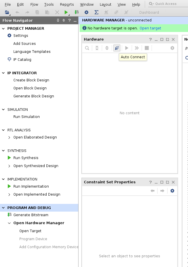
You can select Open Hardware Manger or access it from the left panel.
Proceed and then click the auto connect icon as show in the image:
Right Click the
xc7z100t_0and select Program Device: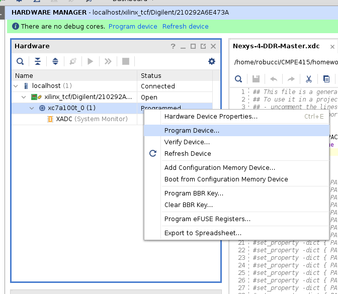
OK-click through the dialogs (the correct .bit progamming file should be found automaticallly) and see if the magic happens. You should be able to connect a VGA monitor and see a Magenta rectangle on a Green Background.
- Connect to Monitor
Connect a VGA cable to the starter board and a monitor. You should see a magenta/purple rectange on a green background.
2. Your Design Assignment
Modify the design to have the ability to change the color of the rectangle based on switch positions.
- The background should be black
- The color of the rectangle should be determined by pressing on one of the four switches SW3,SW2,SW1,SW0 otherwise the rectangle is black.
- The four switches should correspond to magenta, yellow, cyan, and red. Having more than one switch on at a time is a “don't care” condition.
3. Submission (report as ONE PDF file)
- email the TA a report
- TA umbc email: sw33892 Md Rezwanur Rahman (Mahadi)
- Report Requirements:
- one PDF file for entire report
- reasonable, report formatting with very minimal text
- statement regarding completion of assignment (e.g. finished, did not complete…)
- include screenshot of complete top-level schematic
- include before and after of relevant code snippets displaying and explaining changes
- for each of the 5 input states (off,sw0,sw1,sw2,sw3), include
- photograph of FPGA board showing state of switches
- photograph of FPGA board showing computer monitor