# HW 7 VGA Circle
## Objective
In this project students will explicitly implement a computational finite-state machine, utilize rescheduling and resource sharing, and become familiar with the concept of using an on-chip clock multiplier. Students will leverage the faster clock to implement computations in a serial fashion. In this HW students will display a circle on the screen, examine analysis reports, and modify synthesis options.
## Due Dates
* Due Tuesday Dec 12 (Last Day of Class) !!No Late Assignments will be accepted!!
##Description
### 1. To prepare, get your working hw 1 project copied as HW7
### 2. Update UCF
* First, update your ucf to use the TIMESPEC syntax for timing constraints as recommended by XILINX
~~~
# ==== Clock inputs (CLK) ====
NET "CLK_50MHZ" LOC = "C9" |IOSTANDARD = LVCMOS33 ;
# Define clock period for 50 MHz oscillator (40%/60% duty-cycle)
TIMESPEC TS_CLK_50MHZ = PERIOD "CLK_50MHZ" 20 ns HIGH 40%;
NET "CLK_50MHZ" TNM_NET = CLK_50MHZ;
~~~
* Save the text file and close the editor
* Verify the entry is correct by using the Constraints Editor GUI
> * Menu -> Tools -> Constraints Editor
> * You should see something like this
> 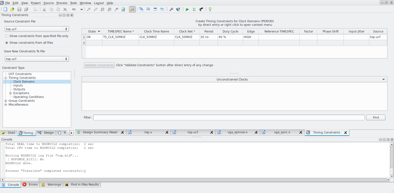
* Close the constraints editor
### 3. Generate a clock multiplier
* Now add a clock multiplier to generate a 100MHz Clock for faster internal computations
* As you've learned before, start to generate an IP Core with "Project -> New Source"
* The module you want to generate this time is a Digital Clock Manager (DCM): FPGA Features and Design -> Clocking -> Spartan-3E, Spartan-3A- > **Single DCM_SP** v13.1
* Options to modify:
* Input Clock Frequency: 50 MHz
* Feedback Value change from 1X to 2X. This enables the CLK2X Output
* Accept the defaults otherwise and process to generating your core
* Inspect the source using "View HDL Source". Notice the use of global buffers and the parameterized DCM_SP module
### 4. Use the Generated 100 MHz clock
* Add the Module to your design using the template found in "View HDL Instantiation Template". It should look something like this:
~~~
// Instantiate the module
myDCM instance_name (
.CLKIN_IN(CLKIN_IN),
.RST_IN(RST_IN),
.CLKIN_IBUFG_OUT(CLKIN_IBUFG_OUT),
.CLK0_OUT(CLK0_OUT),
.CLK2X_OUT(CLK2X_OUT),
.LOCKED_OUT(LOCKED_OUT)
);
~~~
* Modify your designs so the the vga_rectangle uses the CLK2X_OUT (100 MHz) and the vga_sync module uses the CLK0_OUT (50MHz)
* CAREFULLY CHOOSE NAMES FOR THE GENERATED CLOCK NETS AT THE TOP LEVEL VERILOG SO THAT YOU CAN DISTINCTLY IDENTIFY THEM IN REPORTS
* Provide the original 50 MHz clock to the input of the DCM
* Now, verify that the derivative clock constraints exist in your system (they were created by the ip core generator)
* Open the constraints editor GUI "Menu Tools -> Contraints editor"
* Verify that there are TWO NEW TIMESPEC ENTRIES in addition to the orginal
* Each new TIMESPEC should indicate a reference TIMESPEC TS_CLK_50MHZ and Factors *1 for the 50MHz output and /2 for the 100 MHz output
* Verify that the leftmost column "state" is "OK" for both. If either is "Disabled" then something is wrong with your connections
* Add a reset signal to your system and provide it to the DCM (note in simulation that the DCM expects the reset to be asserted for 3 clock cycles)
* Synthesize your design and verify the timing constraints were met. To do this find. Find the following line in your synthesis report
~~~
All constraints were met.
~~~
* Try the design in HW and make sure it shows a rectangle on a VGA screen.
Now Under the Clock Report Section of the synthesis,
Under the Clock Report Section headed with
~~~
/**************************
Generating Clock Report
/**************************
~~~
Find the table that shows SETUP and HOLD Slack "Worst Case Slack" for each clock domain, the 50MHz and the 100MHz.
Include this table along with an interpretation in your REPORT.
### 5. Implement a circle
Now you must implement a 4-stage case-statement-based computational state-machine that tests if a pixel is within 100 Pixels of the center of the screen. Do this by testing to see if the squared distance in pixels is less than 10000. Your state-machine should use the single always block style, and must have the calculations embedded in the sate code.
## 5.1 Single Cycle Computation Design Attempt
* At first try to implement the entire formula (x-xC)^2 + (y-yC)^2 < 10000 in a single line of code. THIS MUST HAPPEN WITHIN ONE STATE OF THE STATEMACHINE (i.e. ONE CLOCK CYCLE). Simulate your module that you have implemented signed arithmetic and have the proper number of bits. Show this test bench and the results in your report.
* Synthesize the design.
* Check the Advanced HDL Synthesis Report "Macro Statistics" to see how many multipliers are included in your design. How many and what types of adders are there? How many comparators and of what size? Include the "Macro Statistics" in your REPORT along with discussion.
* Now, find the section that shows the FSM State Encoding. Include this in your REPORT and discuss how it is different than the encoding your provided in your code.
* Finally, verify that your design does not meet timing constraints. Find the line in the report stating that a contraint was NOT met. Include this in your report along with other information you find in the report related to the cause of the failure. What are the timing slacks? If by chance your does meet all contraints, please see me before submission.
## 5.2 Multiple clock cycle computation Design with Resource Sharing
* Now, implement the computational FSM deign in such a way that it only uses one multiplication at a time. As your break up your computation, be careful that you are casting to signed and have the appropriate number of bits for each partial result (reg). To suggest resource sharing make sure that the multiplication operation is isolated and that it only writes to the exact same named variable. You'll have to work your other code around this.
* Verify that your new design only has 1 multiplier and meeting timing constraints. Provide the Macro Statistics and discuss in your REPORT. Also, include the timing slack analysis results for each clock domain in your REPORT.
* Finally discuss if you see this line is in your report:
~~~
All constraints were met.
~~~
* Be sure to test your synthesized design in hardware and report your level of success in your REPORT.
## 5.3 Multiple clock cycle computation Design WITHOUT Resource Sharing
* Disable resource sharing in the synthesis options
* with "Synthesize - XST" selected, goto process properties in the menu "Process -> Process properties..."
> 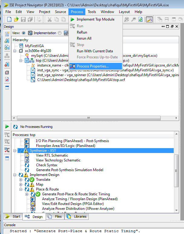
* under HDL Options find **-resource_sharing** and uncheck it
* While you are looking at synthesis options, notice that you can turn off use of specialized hardware and instead set -mult_style to use LUTs. (DON'T DO THAT JUST HAVE A LOOK AT THE OPTION)
* Resynthesize your design.
* Look at your "Macro Statistics" Report in your synthesis report. Verify that 2 multipliers are there and discuss in your report. Include the Macro Statistics and are discussion of the statics in your REPORT. Also include timing slack analysis results.
* Be sure to test the implementation in hardware.
-