Metastabilty
Ryan Robucci

• ESC/O-Key to see slide overview • ? to see help
 Printable Version
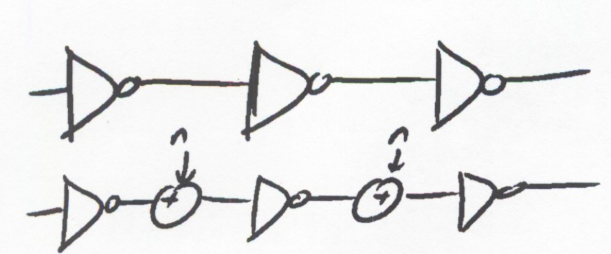
Digital Abstraction and Noise
- consider a chain of digital gates
- signal corruption model: ideal gates with noise sources
- desire proper interpretation of binary values in presence of noise
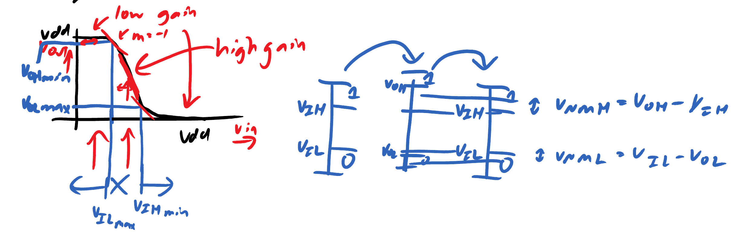
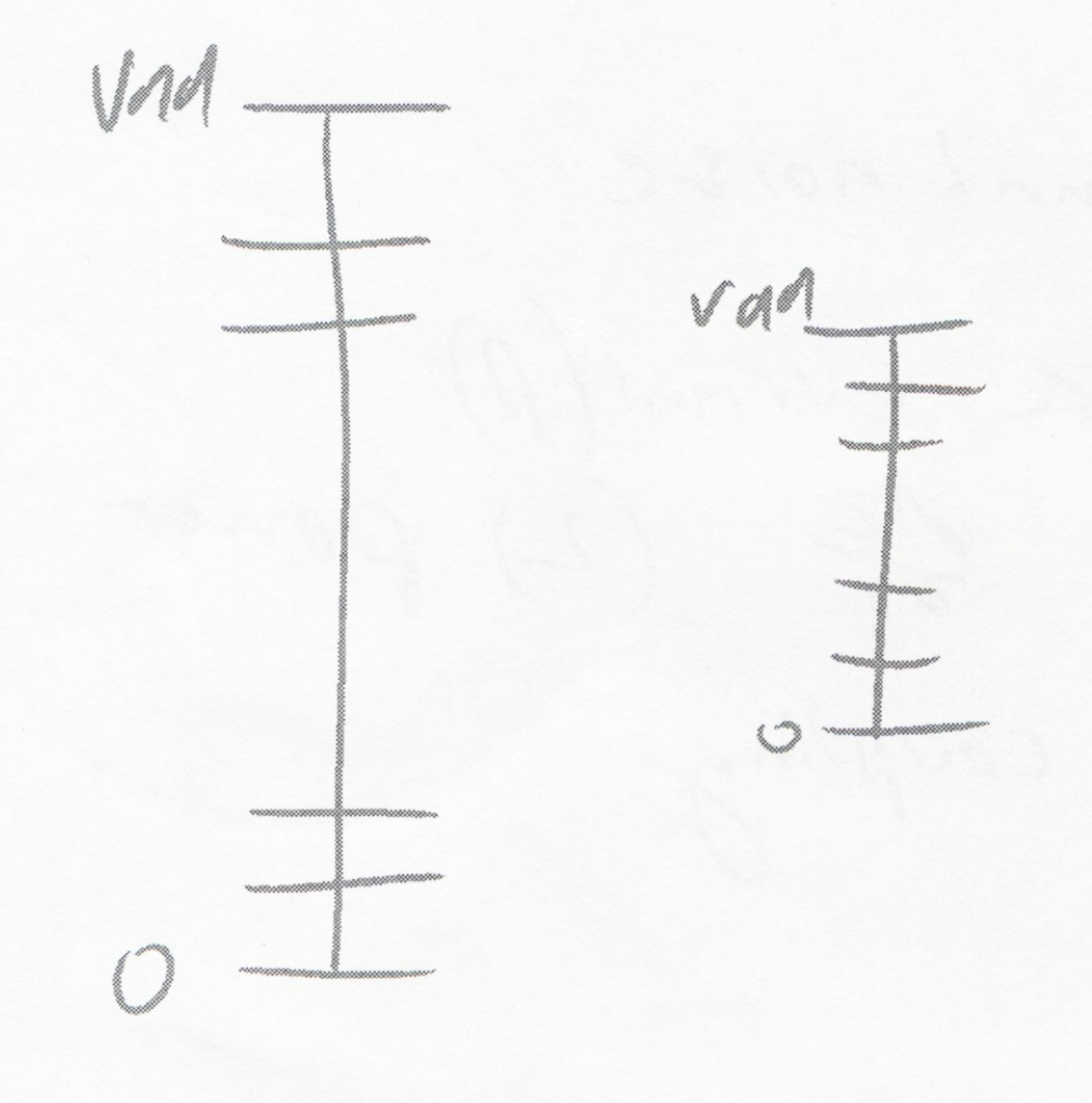
- Noise Margin High is the margin for
'1' - Noise Margin Low is the margin for
'0'
Noise F.O.M.
- Some corruption is proportional to voltage swings
- Examples:
- larger transition -> larger ringing
- larger transition -> larger disturbance on neighboring signal lines
- Examples:
- Noise Performance Figure of Merit: Ratio of Noise Margin to Voltage Swing is a useful figure of merit (FOM)
For example: for two logic families, noise margins that are proportional to the power supply level may perform roughly the same
or
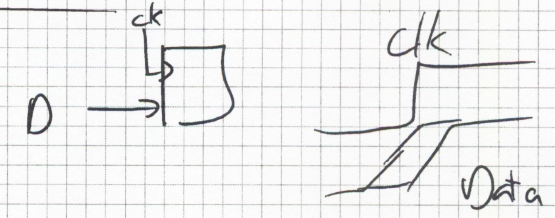
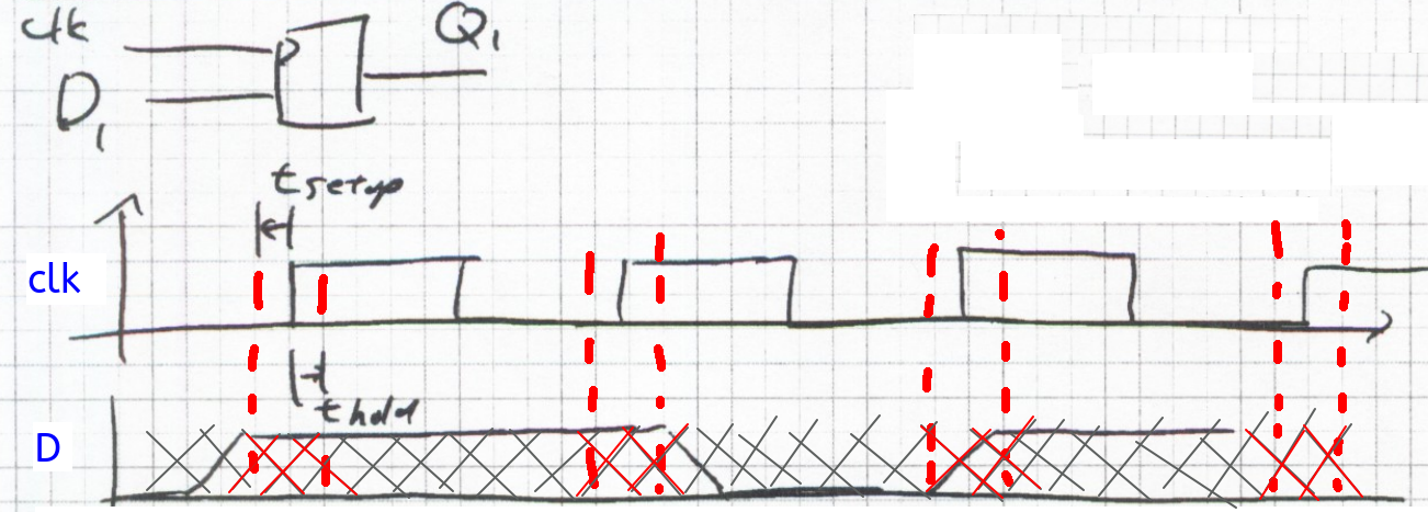
Timing Requirements for Registers
- Registers tend to have voltage as well as specific timing requirements for the inputs
- Setup and Hold
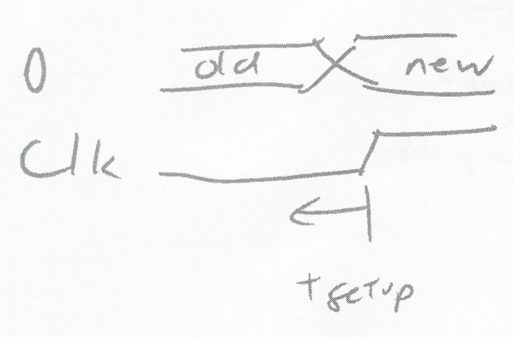
- If violated, may get
- Old Data
- New Data
- Metastable Output
- Not conform to voltage specifications
- May change in middle of clock period (multiple output transitions triggered by the clk)
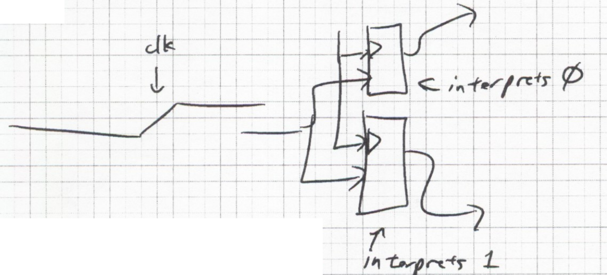
Possible Output transitions when expected is 0->1:

Clock Domain Crossing
- Clock Domain Crossing arises from the need to communication between Multiple Clock Domains
- You have learned in sync. design in one clock domain
- Having Multiple Clock Domains means Clock Domain Crossing must be considered
Async Inputs
Not all signals arise from a clock domain at all, such as physical, real-world inputs
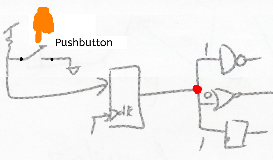
A problem arises at a fanout point, where mutiple interpretations are performed in parallel
Metastabilty
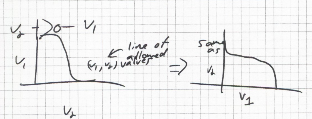
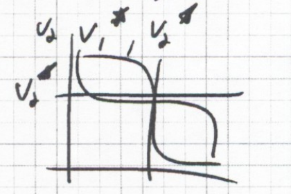
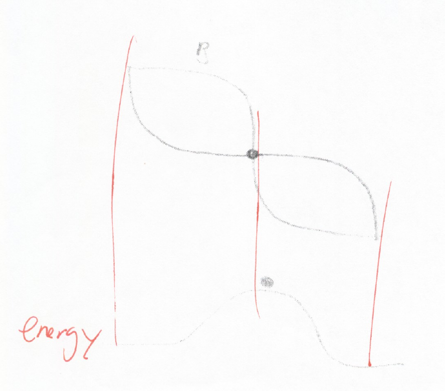
Consider that an inverter represents contrain on allowed input, output (,) relationships:
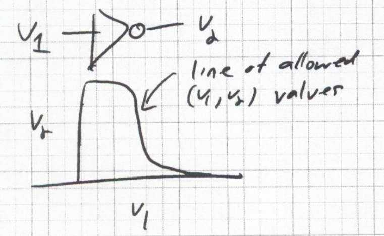
Consider another inverter with the input and output connections reversed:
Consider a coupled set of inverters, setting constraints between V1 and V2
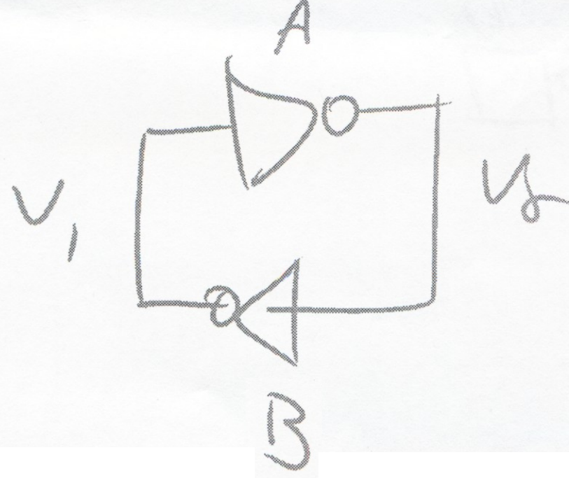
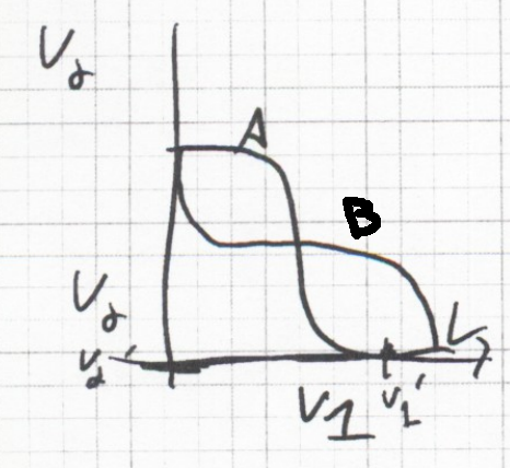
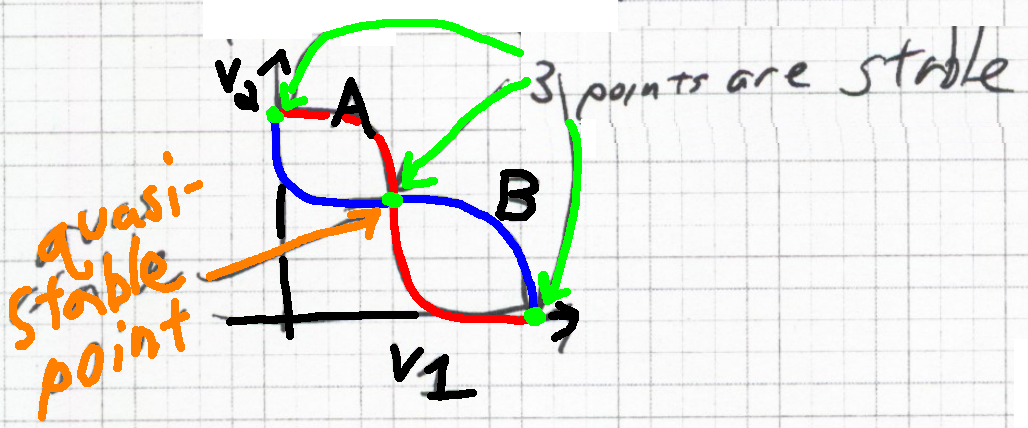
Two constraints, A and B
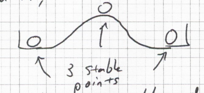
Three Points are possible solutions to both constraints
1 is a quasi stable solution
Temporal Dynamics Analysis
Time analysis:
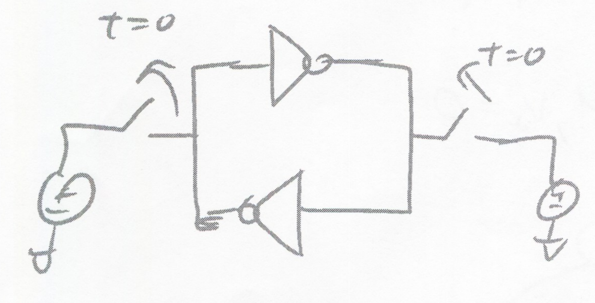
Consider ideal voltage sources and switches set two intial voltages
Switches are opened at time t=0
Case Quasistable:
In theory, the middle point is also stable
We have assumed a symmetric transfer function and constraints
However, any noise will disrupt the balance.
If is bumped more positive, is pushed more negative and thus is pushed more positive, etc...
Positive Feedback ensure until and
Quasi-stable
-
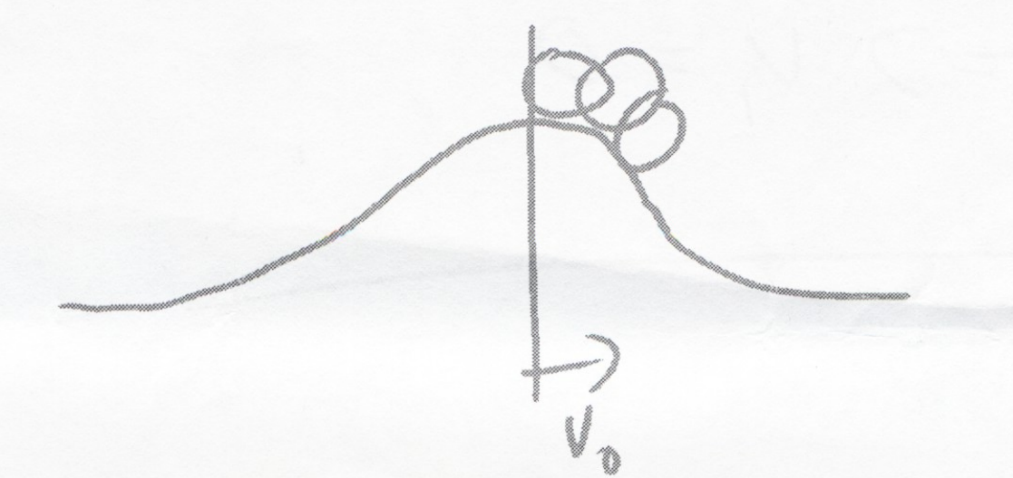
Think of of the quasi-stable point in the analogy of balancing a ball on a hill:
-
Middle point is quasistable and can only be preserved in a noiseless system. Starting points to the left of middle are pushed towards the left and starting points on the right are pushed to the right
-
Maintaining Highest Potential Energy:
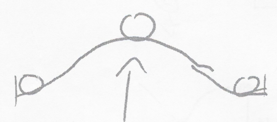
Quasi-stable point can only be preserved in a noiseless system
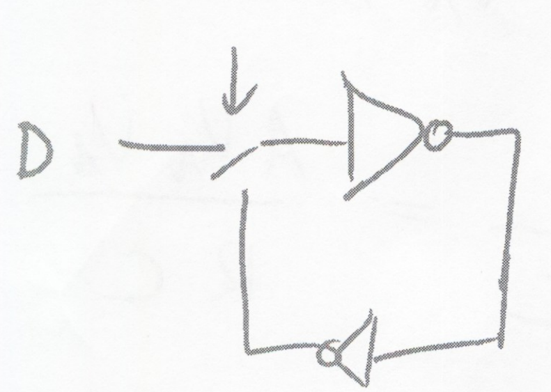
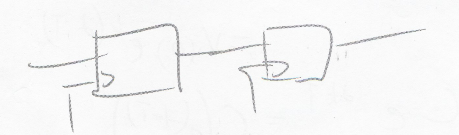
SRAM
Two Inverter (SRAM):
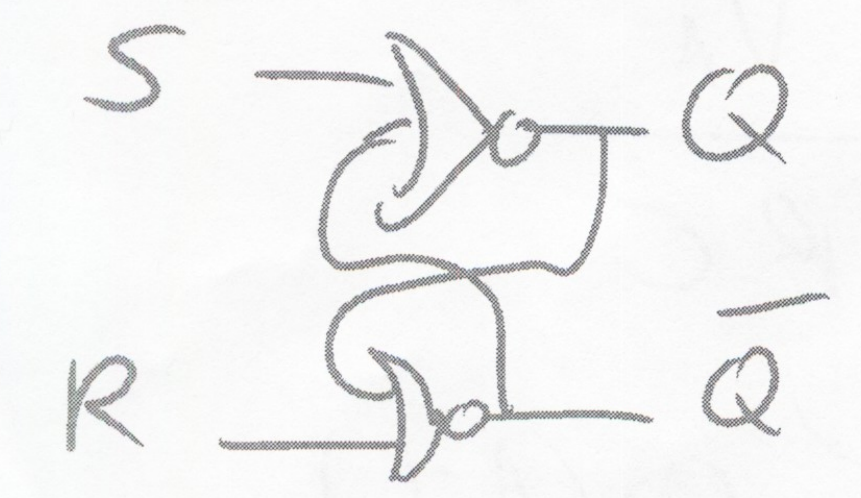
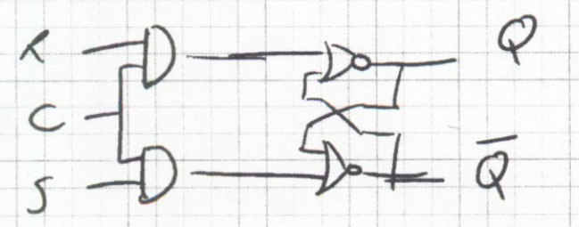
S-R Latch:
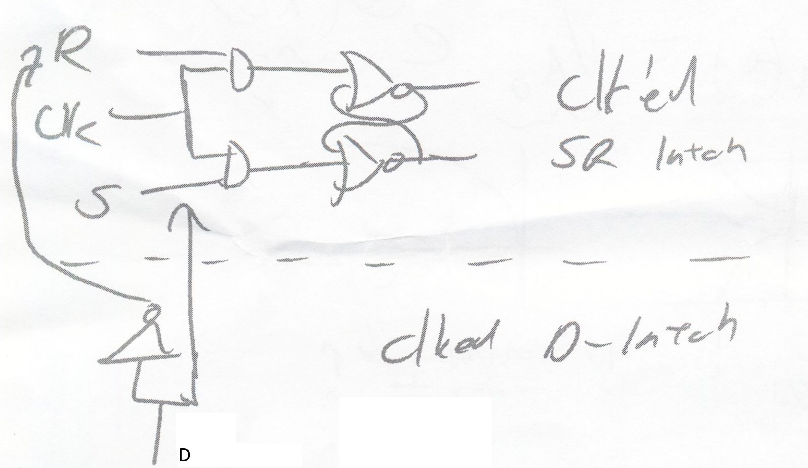
Clocked (Level Sensitive) SR Latch
Clocked D-Latch:
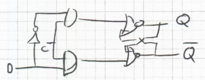
alternative view as extension of clocked SR latch:
Time to Settle
The question of interest is how long does is take to reach a stable state as a function of starting position?
Given how long to reach a stable point?
Given T, a time limit to reach stable point, what is the constraint on ?
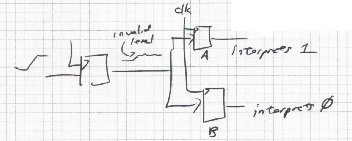
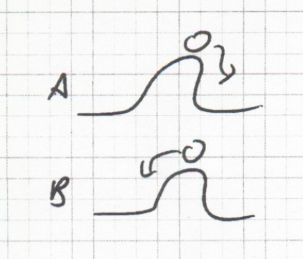
Metastable Cause
Clocked latches can be placed near a metastable state if the clock transistions while data is
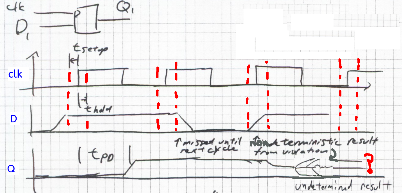
The problem is more than complex than "will it settle to the new or old value?"
If placed in a metastable state, the output can be stuck near the quasistable point for a very long time and the following stages will non-deterministically interpret the signal as 1 or 0 depending on thesholds and noise
- Latches are vulnerable to corruption when they are in a state near the quasi-stable point
- Transitions disrupted at the wrong time can be delayed reversed, or even undergo multiple transitions
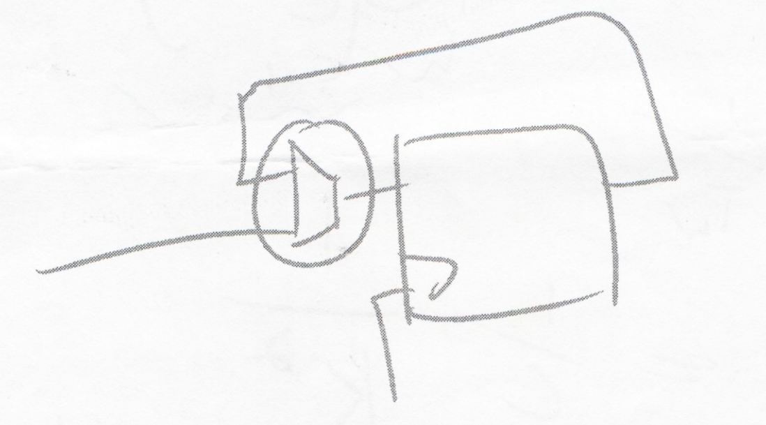
Synchronized Input Capture:
Assume in the Logic, D1 and D2 represent two conditions that are normally never true but are often opposite in value. This logic is checking if the condition that D1 and D2 are ever true together
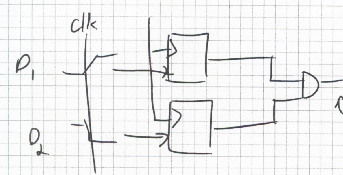
Here the output may glitch or become high in error under normal conditions, such as simutanuous tranistions D1: and D2:
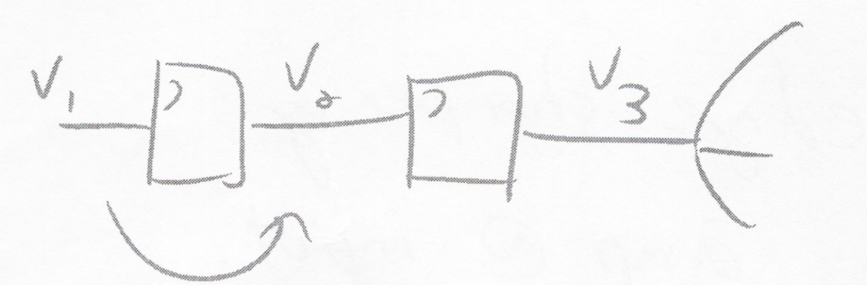
Resolution Fanout Point
At some point in the system, parallel resolution must happen that can cause a problem
The same input signal (staring point) can be resolved differently in two components
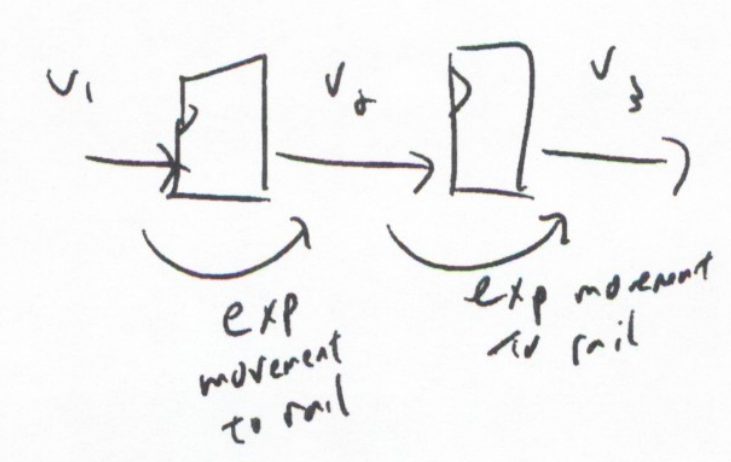
Temporal Analysis
A generic representation of positive feedback:
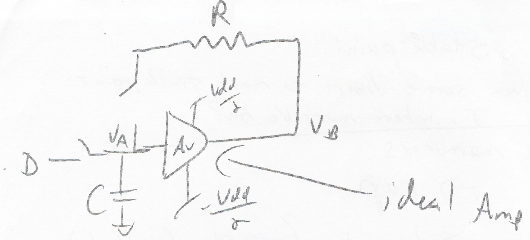
Assume the Ideal Amp, at all times
Positive Feedback
General behaviour of positive feedback is to accellerate away from a quasi stable point (VA=VB=0)
Negative feedback for comparison:
fast than slow settle at a equilibrium
Analysis
Analyze the temporal voltage change at the input storage capacitor. The voltage value here represents the state of the system
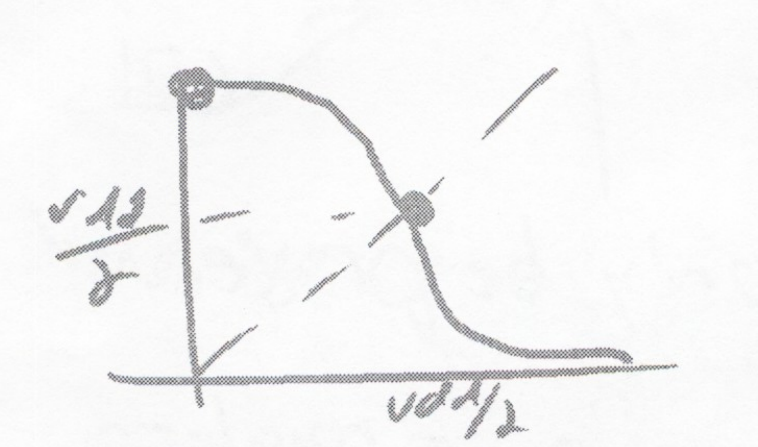
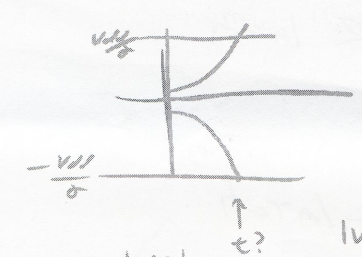
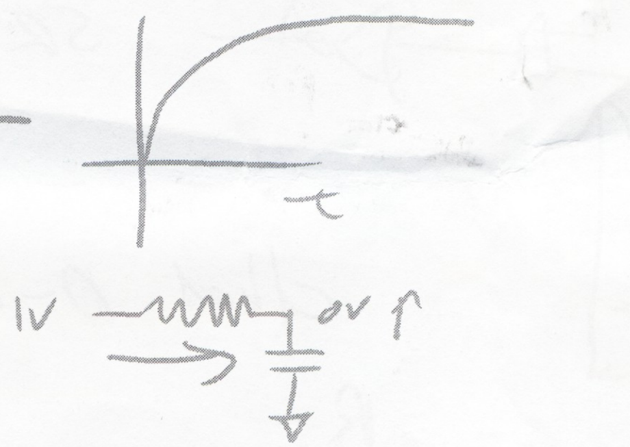
Time and Voltage Constraint
Bound t to be less than a desired clk-to-Q, i.e. time to resolve, , and find
and here represent the time and voltage constraints on the input
-
Starting values farther from the metastable equilibrium than will resolve quickly
-
Starting values closer to the metastable equilibrium than will resolve in a much longer amount of time, and meanwhile are more susceptible to noise corruption
-
Nature of Exponentials (Self-similartity)
- Leads to linear input voltage -> exponential settling time relationship
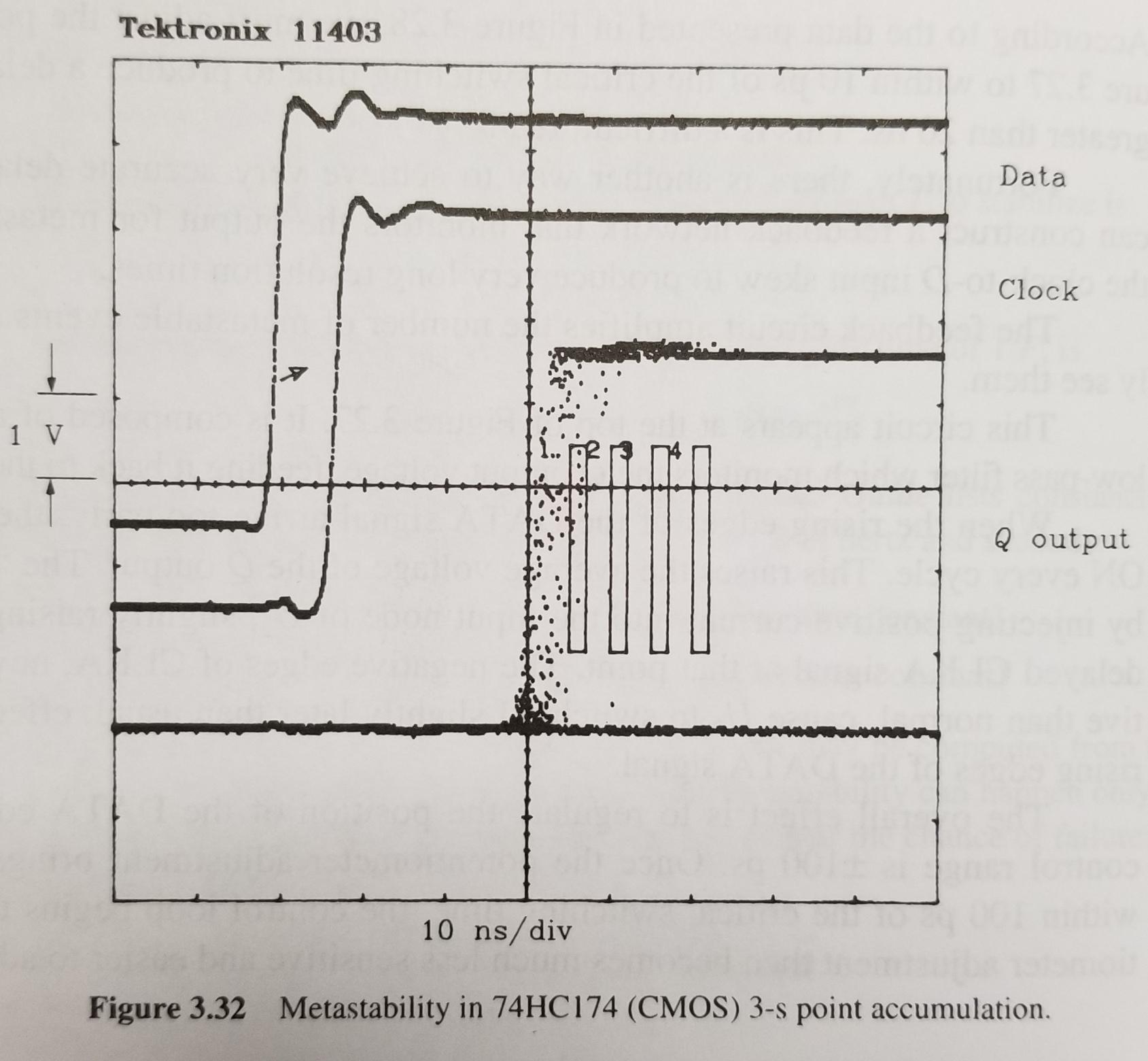
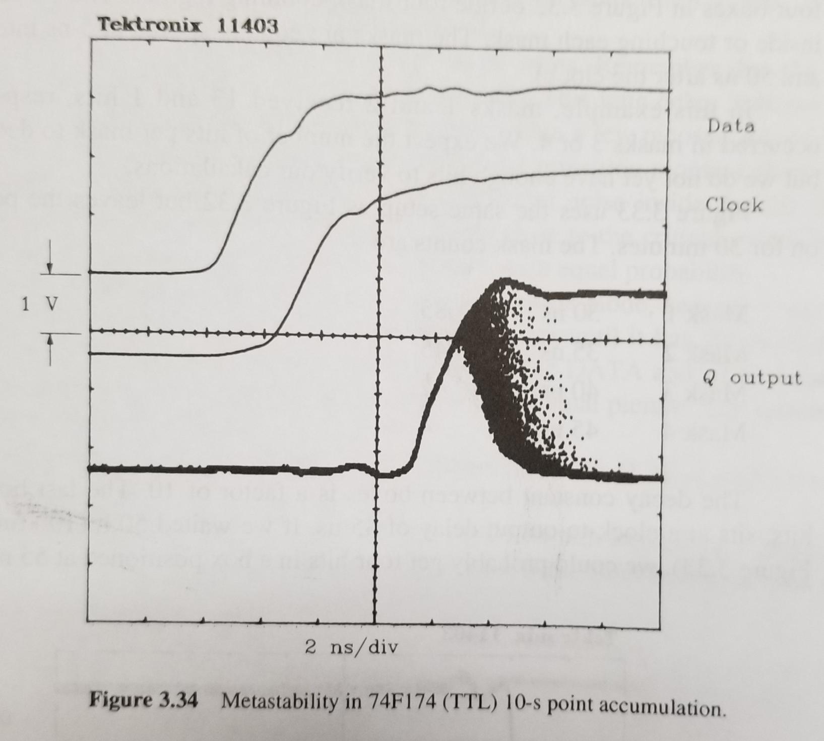
- See the mask counts on the next page for 30-min accumulation:
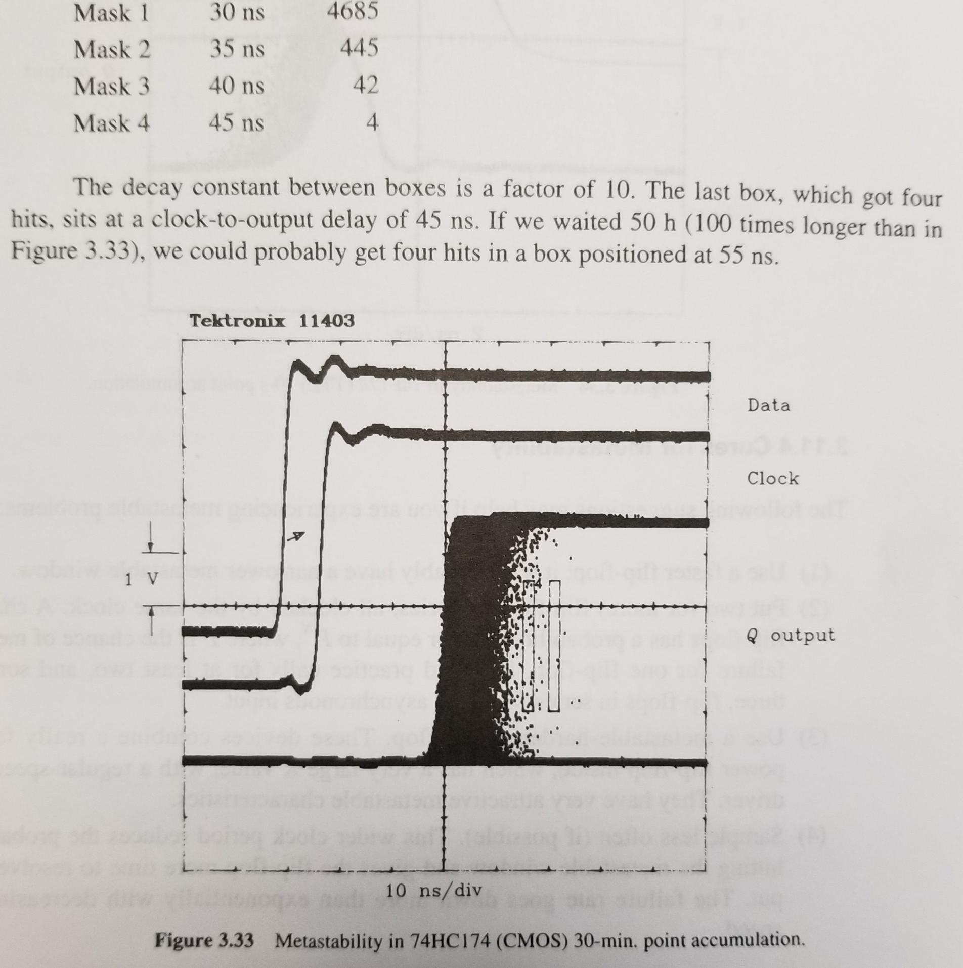
Implication of Metastabilty
For a given rise time, an input transition must stay outside a time window around the clock event
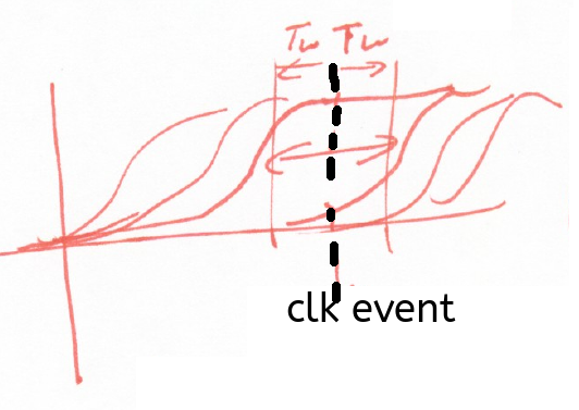
Implications of data transition slope and timing
The rise time and allowed arrival time of a 50% transition point are related
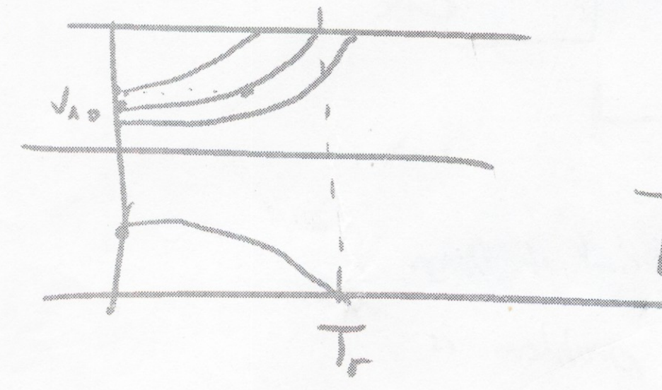
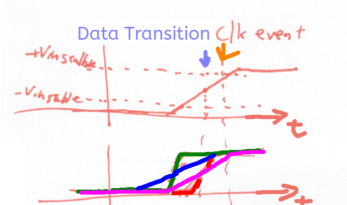
Data as Reference
For the next analysis: instead of viewing the clk as the reference and data timing as the variable:
We will switch and consider the data edge to be the transition
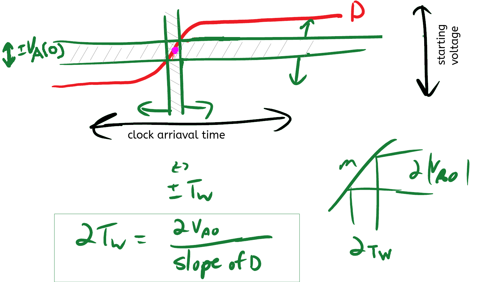
- If clock rises in in the data window, the output may not settle in time [eq 3.34]:
- C is a constant (maybe found empirically), rise-time is a primary component
System Timing Requirements
is the window of error [eq 3.36] that helps define setup and hold time requirements and thus allowed combinatorial propagation delays
Operation Timeline
- Assume a uniformly random arrival of Data:
- Chance of MS Problem is [3.37]
- Probability of Failure Per Data Transition:
(this is the likelihood that a random transition falls in a disallowed epoch)
- When looking at various documents and datasheets, you may see many alternative forms but with similar underlying form
Actel 1989 ACT-1 Logic:
- Sample Switch Rise Time Constant
- Response Time Constant
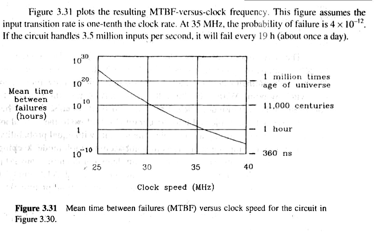
Page 127
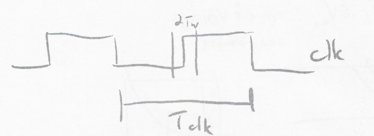
R (rate of transitions) is 1/10th of the clock rate
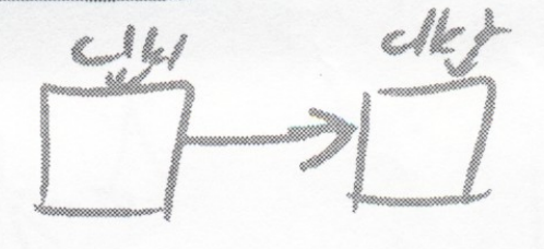
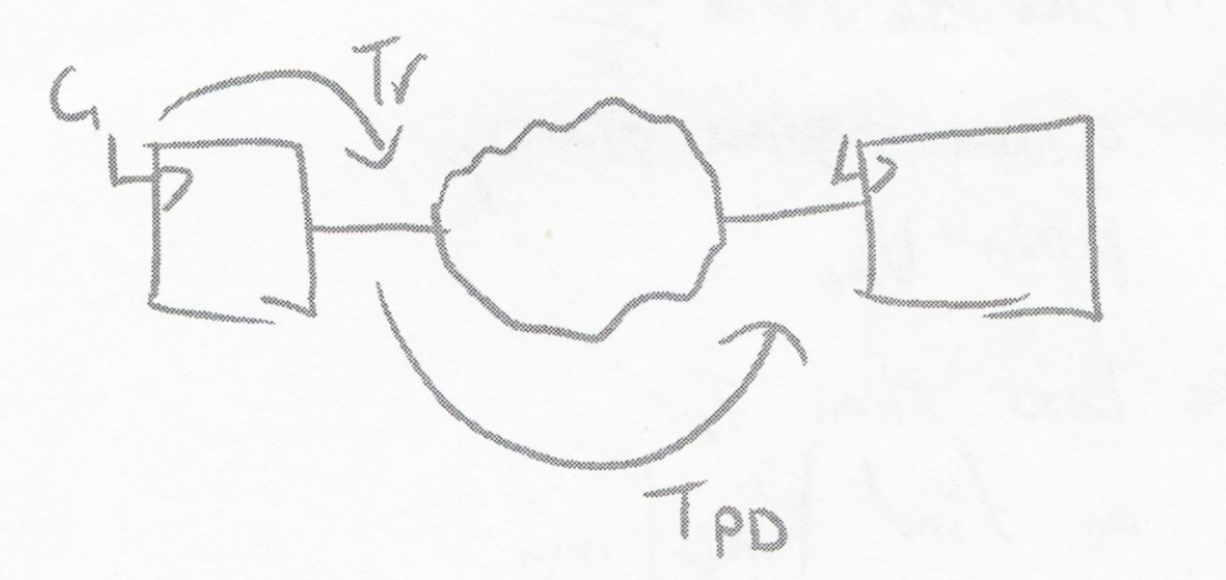
- N-FlipFlops in a row:
Effective Time provided is doubled (2T):
for 2 flip-flops
for N flip-flops
Another Possibility to realize this effect for a multi stage (e.g. master-slave) flip-flop: