Multi-clock/Async Communications and Clock Management
Ryan Robucci

• Spacebar to advance through slides in order
• Shift-Spacebar to go back
• Arrow keys for navigation
• ESC/O-Key to see slide overview • ? to see help
• ESC/O-Key to see slide overview • ? to see help
 Printable Version
Example of bad clock distribution
- Imbalanced (systematic/design)
-
Balanced
-
Remeber, clock skew matters, delay may be OK if balanced
Multiple Clock Domains
-
Many digital systems have more than one clock domain:
-
Need to synchronize the two clock domains, two basic building blocks:
- Phase-locked loop (PLL)
- Delay-locked loop (DLL)
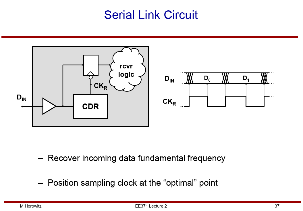
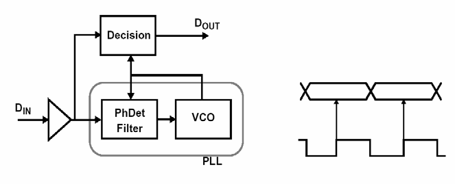
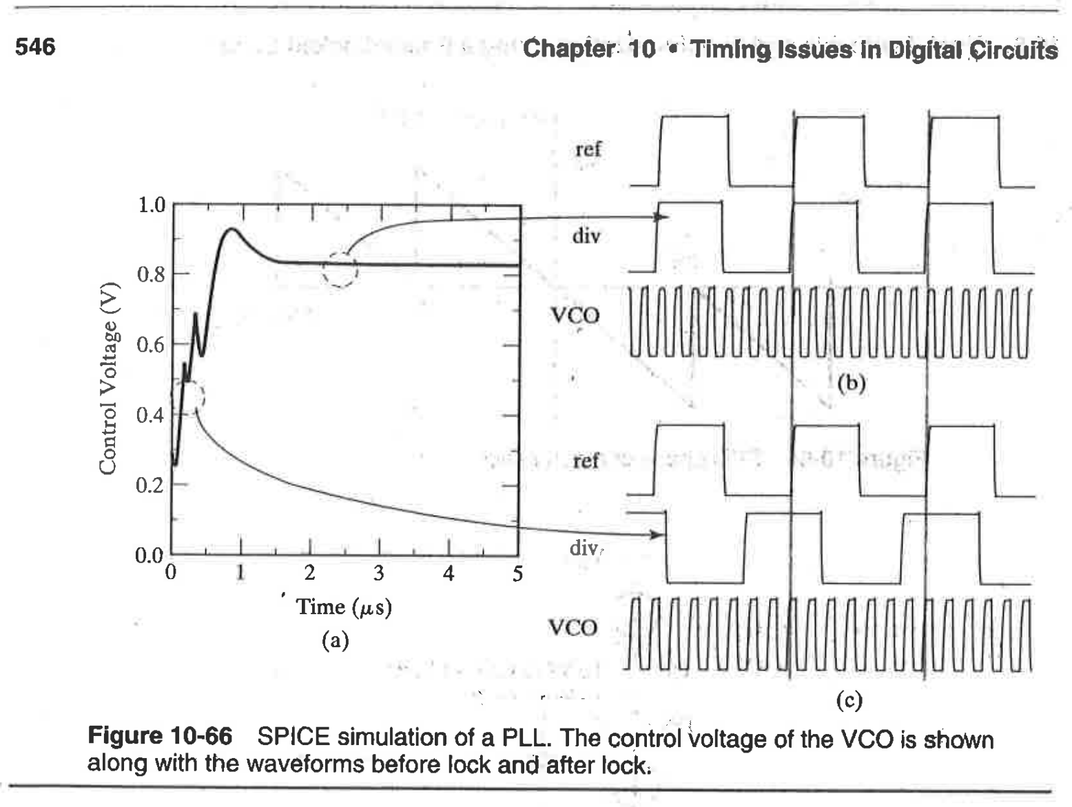
Example: Classical clock recovery
- Clocking information embedded in data stream
- Use PLL to recover the clock
- State of system is stored in analog loop filter
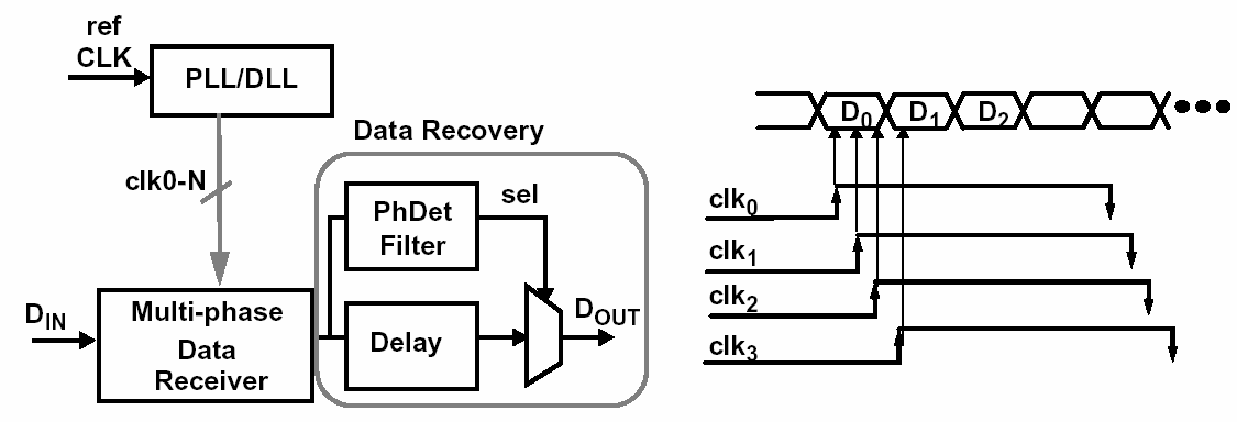
Oversampled Clock/Data Recovery
- Oversample the data and perform phase alignment digitally
- De-couples clock generation from tracking of data
- Data must guarantee transitions (edges) to ensure tracking
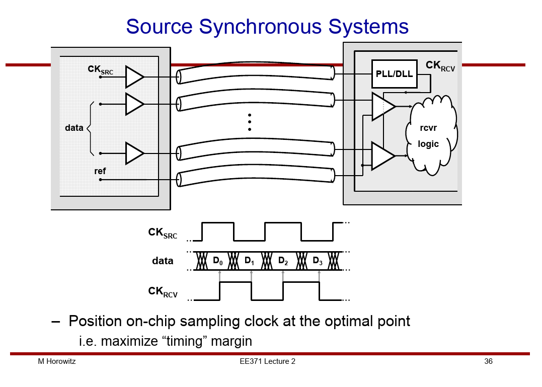
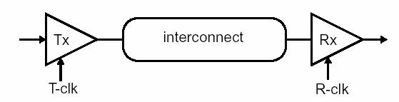
Phase Alignment in Source Synchronous Systems
- Timing information carried by reference clock
- Use DLL to ensure proper clock phase for sampling
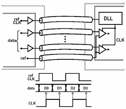
- Can correct for skew using DLL or PLL
PLLs and DLLs
https://www.xilinx.com/support/documentation/application_notes/xapp132.pdf
- DLL: based on a variable delay line based on voltage controlled delay (analog) or a chain of delay elements with selectable output tap along the chain
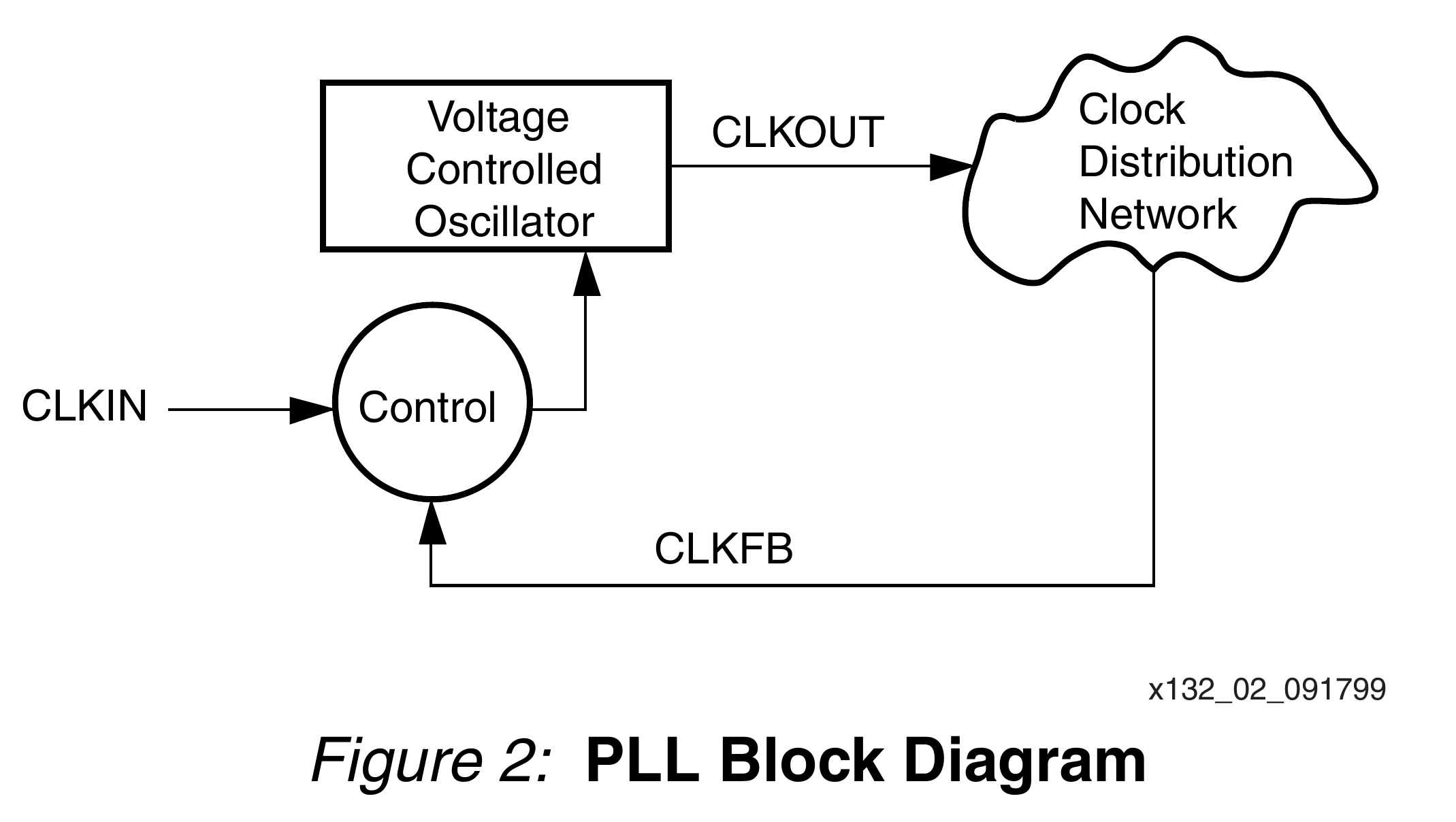
- PLL: based on a variable (voltage controlled) ocilator,
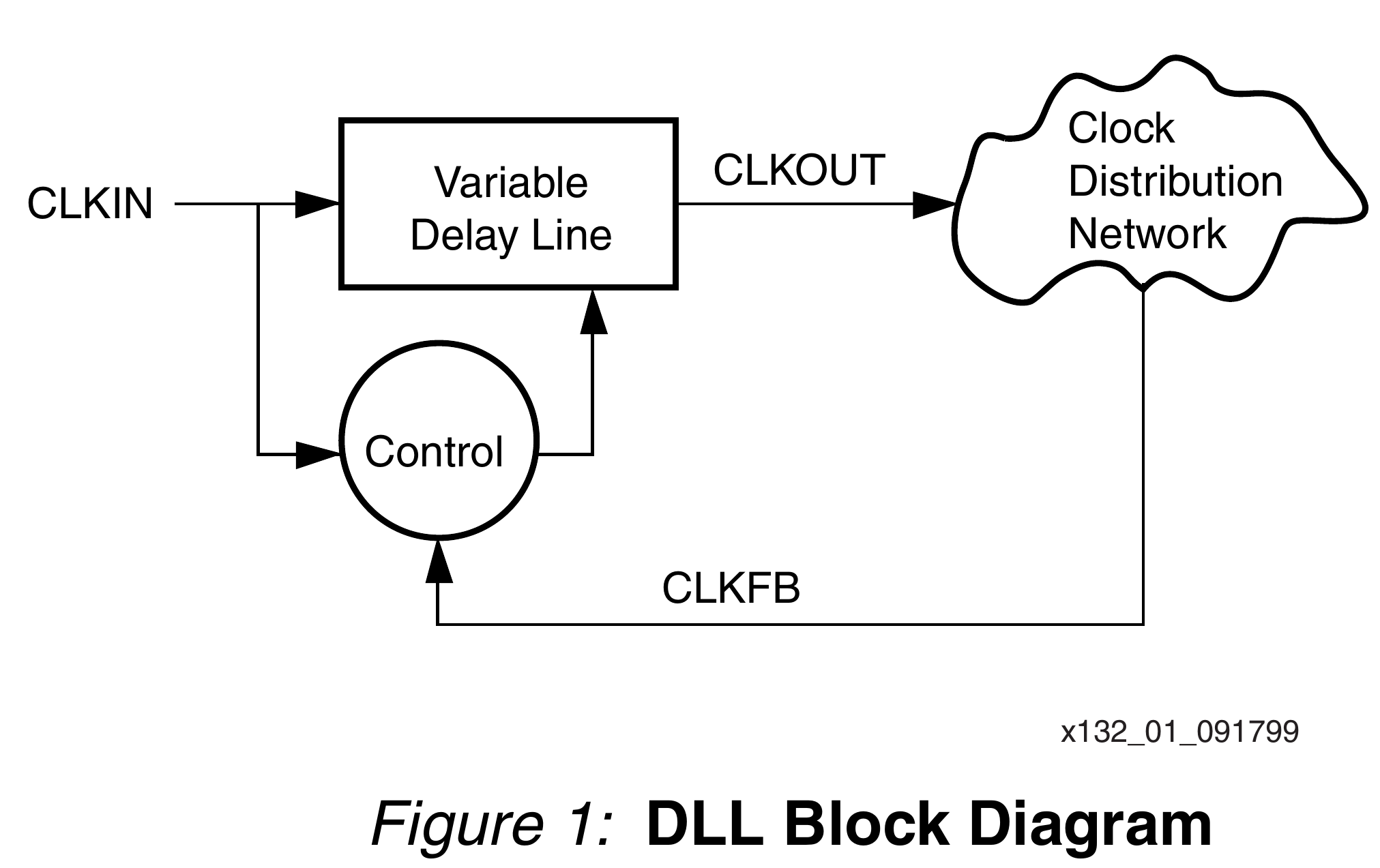
What is a Delay locked loop?
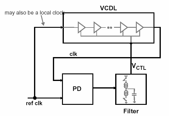
- based on delaying input reference clock, so reference clock jitter passes to output
- no phase error accumulation
- frequency synthesis is difficult, PLL is well-suited for this
Typical Loop Filter
A “charge-pump” acting as an ideal integrator
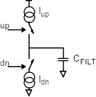
- Incremental update signals increase or decrease charge over many cycles
Typical Osscilation/Delay Elements
(oscillator shown)
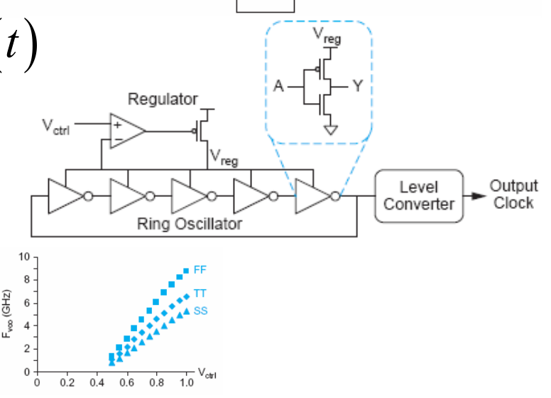
- tunable capacitance, resistance, and current drive are all possible
What is Phase locked loop?
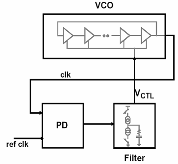
- frequency multiplication is easy
- can perform frequency synthesis according to ratio of integers
- reference clock jitter reduced by filtering
- suffers phase error accumulation
Use of a divider for Freq Multiplication
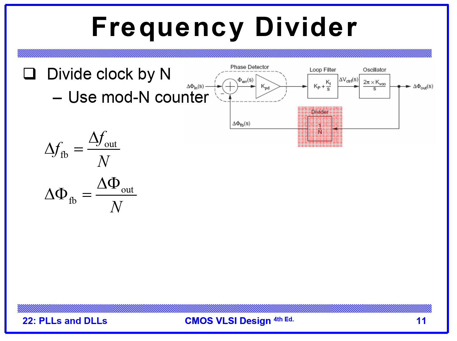
- ignoring the initial locking procedure, by keeping every n-th edge in sync with the reference we can achieved a synchronized, higher-freq clock
(Rabaey et al.)
Linear Phase Detectors
-
Correction signal is linearly proportional to error
-
XOR phase detector - 90
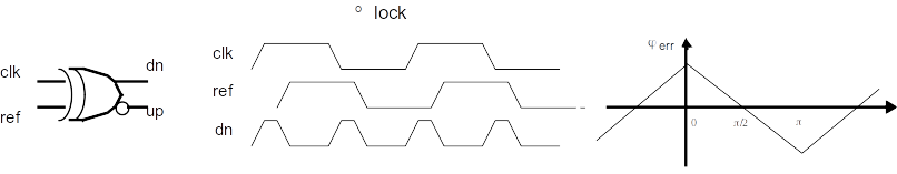
- sensitive to input duty cycle
-
SR phase detector - 180
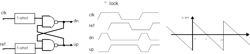
- 1-shots remove duty cycle sensitivity
Non-linear Phase Detector [EE 371 Lecture 17 29]
- An ideal flip/flop should force a loop to lock at 0
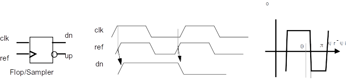
- The set-up time of the flip-flop will introduce phase offset
- Symmetric structures can eliminate this problem [16]
- Can be used to cancel the set-up time of an input sampler [13]
Timing Loop Performance Parameters
- Phase Jitter:
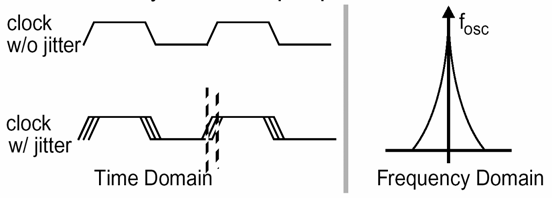
Varience in cycle to cycle clock period
Related to ability to "filter" reference clock jitter (which could be desired or not) - Phase Offset: Error between output phase and reference phase
Zero Delay Buffer

DLL in Xilinx Virtex data/clock alignment
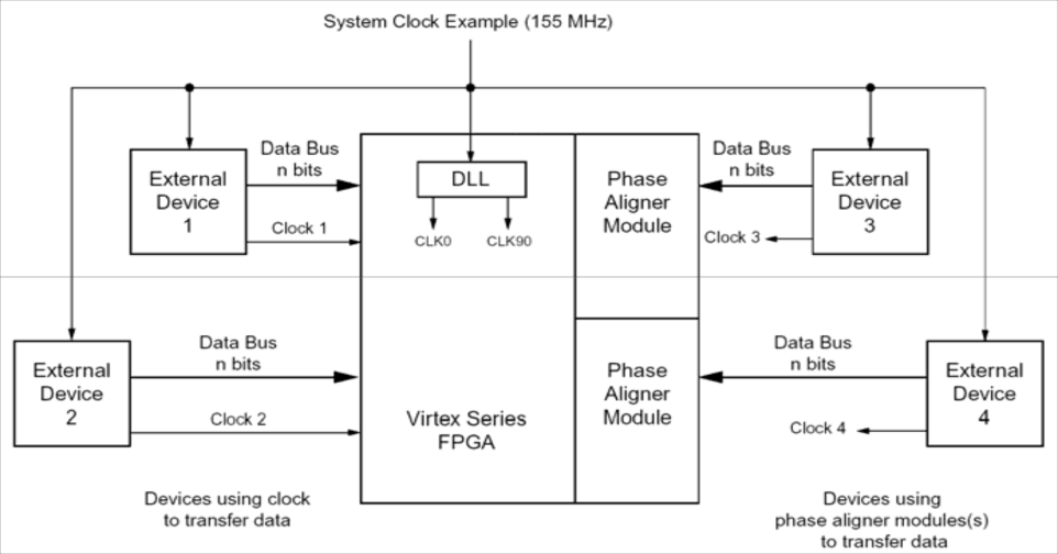
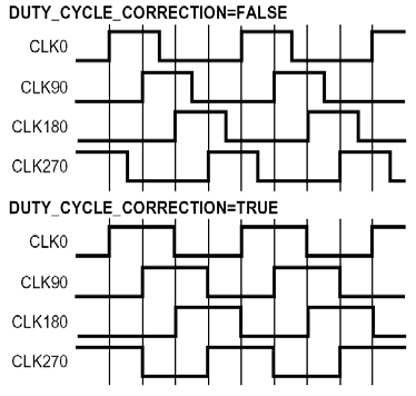
Xilinx DLL with various phase outputs
- DLLs are commonly used to generate outputs at the same frequency but different phases, just by having multiple taps along the delay line


Using DLL to de-skew onboard clock signals
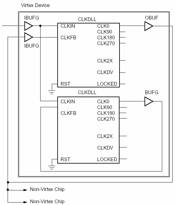
- FPGA can drive external clocks, and by passing back an external (board level) reference signal they can be adjusted to match a reference clock (at a known phase)
- This compensates for unknown loads (common to see with external memory ICs)
Altera Cyclone II PLL (1)
- Phase-locked loop (PLL) is a closed-loop frequency-control system based on the phase difference between the input clock signal and the feedback clock signal of a controlled oscillator.
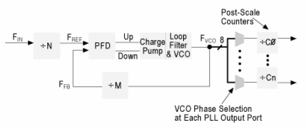
Altera Cyclone II PLL (3)
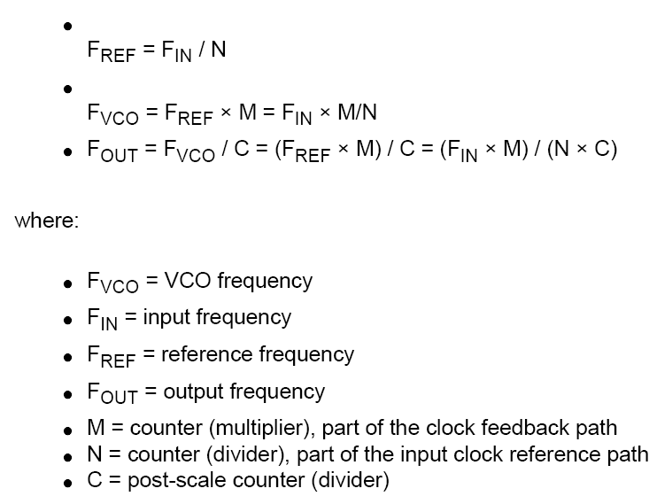
- The output frequency is given by:
UART
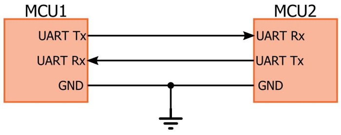
- UART: universal asynchronous receiver/transmitter
- basic UART system provides robust, moderate-speed, full-duplex communication with only three signals: Tx (transmitted serial data), Rx (received serial data), and ground. In contrast to other protocols such as SPI and I2C, no clock signal is required because the user gives the UART hardware the necessary timing information.
- Internal “clocks” of systems must be synchronized based on the data signal
- System must both know the approximate clock rate and generate internal clocks
- The error in the rates must be low enough to assume synchronization for one frame, so frame are kept short (<10 bits)
Start and Stop bits
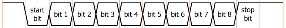
- Start bit: The first bit of a one-byte UART transmission. It indicates that the data line is leaving its idle state. The idle state is typically logic high, so the start bit is logic low.
- The start bit is an overhead bit; this means that it facilitates communication between receiver and transmitter but does not transfer meaningful data.
- Stop bit: The last bit of a one-byte UART transmission. Its logic level is the same as the signal’s idle state, i.e., logic high. This is another overhead bit.
Buad Rate
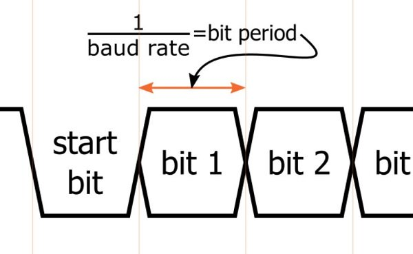
- Baud rate: The approximate rate (in bits per second, or bps) at which data can be transferred.
- A more precise definition is the frequency (in bps) corresponding to the time (in seconds) required to transmit one bit of digital data.
- For example, with a 9600-baud system, one bit requires 1/(9600 bps) ≈ 104.2 µs. The system cannot actually transfer 9600 bits of meaningful data per second because additional time is needed for the overhead bits and perhaps for delays between one-byte transmissions.
Synchronizing and Sampling
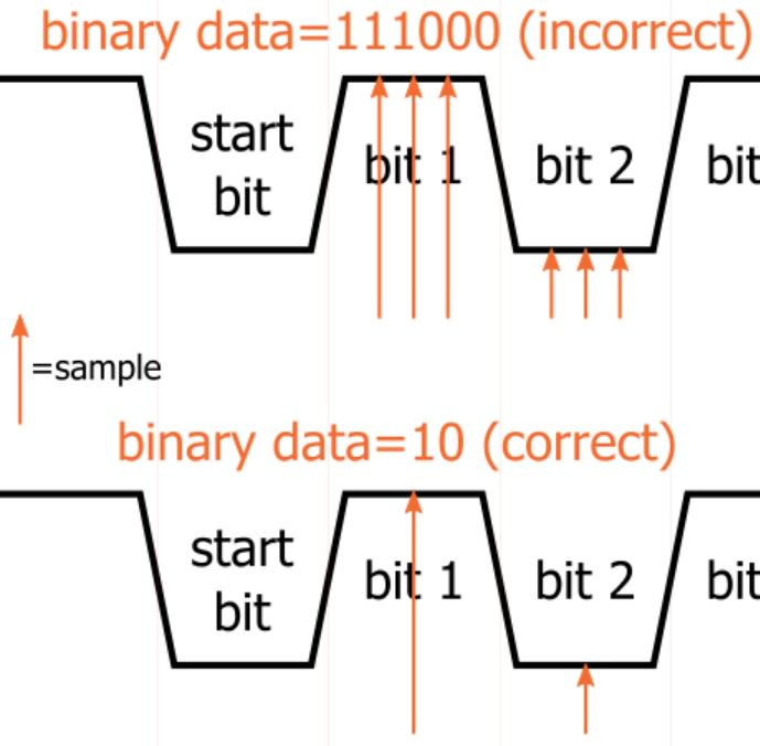
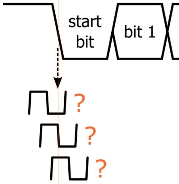
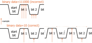
- To ensure that an active edge of the receiver clock can occur near the middle of the bit period, the frequency of the baud-rate clock sent to the receiver module is much higher (by a factor of 8 or 16 or even 32) than the actual baud rate.
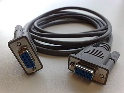
RS232
-
RS232 Standard specifies voltages and hardware connectors
 https://et.wikipedia.org/wiki/RS-232
 -
Commonly referenced and emulated communication, e.g. USB-to-Serial
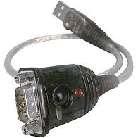 https://www.cdw.com/product/Iogear-16.6in-USB-to-Serial-RS-232-Adapter/261218